ADL5567
新規設計に推奨4.3 GHz, Ultrahigh Dynamic Range, Dual Differential Amplifier
製品の詳細
- −3 dB bandwidth of 4.3 GHz
- High performance (HP), low power (LP), and power down modes
- Preset 20 dB gain can be reduced by adding external resistors
- Channel to channel gain error: 0.04 dB at 500 MHz
- Channel to channel phase error: 0.6° at 500 MHz
- Differential or single-ended input to differential output
- Internally dc-coupled inputs and outputs
- Low single-ended input distortion
- Slew rate: 20 V/ns
- Low noise input stage: 7.4 dB noise figure at 500 MHz
- Low broadband distortion for supply = 5 V, HPmode, and 2 VP-P
- 200 MHz: −94 dBc (HD2), −103 dBc (HD3)
- 500 MHz: −82 dBc (HD2), −82 dBc (HD3)
- Maintains low distortion for output common-mode voltage down to 1.25 V
- Single-supply operation: 3.3 V or 5 V
- Low dc power consumption: 148 mA at 5 V (HP mode), and 80 mA at 3.3 V (LP mode)
The ADL5567 is a high performance, dual differential amplifier optimized for intermediate frequencies (IF) and dc applications. The amplifier offers a low noise of 1.29 nV/√Hz and excellent distortion performance over a wide frequency range, making it an ideal driver for high speed 16-bit analog-to-digital converters (ADCs). The ADL5567 is ideally suited for use in high performance zero-IF and complex IF receiver designs. In addition, this device has excellent low distortion for single-ended input driver applications.
The ADL5567 provides a gain of 20 dB. For the single-ended input configuration, the gain is reduced to 18 dB. Using two external series resistors for each amplifier expands the gain flexibility of the amplifier and allows for any gain selection from 0 dB to 20 dB for a differential input and 0 dB to 18 dB for a single-ended input. In addition, this device maintains low distortion down to output common-mode levels of 1.25 V, and therefore providing an added capability for driving CMOS ADCs at ac levels up to 2 VP-P.
The quiescent current of the ADL5567 using a 5 V supply is typically 74 mA per amplifier in high performance mode. When disabled, each amplifier consumes only 3.5 mA, and has 58 dB input to output isolation at 100 MHz.
The device is optimized for wideband, low distortion, and low noise operation, giving it unprecedented performance for overall spurious-free dynamic range (SFDR). These attributes, together with its adjustable gain capability, make this device the amplifier of choice for driving a wide variety of ADCs, mixers, pin diode attenuators, SAW filters, and multielement discrete devices.
Fabricated on an Analog Devices, Inc., high speed silicon germanium (SiGe) process, the ADL5567 is supplied in a compact 4 mm × 4 mm, 24-lead LFCSP package and operates over the −40°C to +85°C temperature.
APPLICATIONS
- Differential ADC drivers
- Single-ended to differential conversions
- RF/IF gain blocks
- SAW filter interfacing
ドキュメント
データシート 1
技術記事 1
製品選択ガイド 1
Analog Dialogue 1
これは最新改訂バージョンのデータシートです。
ソフトウェア・リソース
必要なソフトウェア/ドライバが見つかりませんか?
ドライバ/ソフトウェアをリクエストツールおよびシミュレーション
ADIsimRF
ADIsimRFは使いやすいRFシグナル・チェーン計算ツールです。最大50段までのシグナル・チェーンについて、カスケード・ゲイン、ノイズ、歪み、消費電力を計算し、プロット、エクスポートが可能です。ADIsimRFには、アナログ・デバイセズのRFおよびミックスド・シグナル部品のデバイス・モデルの広範なデータ・ベースも含まれています。
ツールを開くキーサイトGenesys向けのSys-Parameterモデル
Sys-Parameterモデルは、デバイスの直線性と非直線性を明らかにするP1dB、IP3、ゲイン、ノイズ指数、リターン損失などの挙動パラメータを提供します。
ツールを開く評価用キット


ADL5567 & AD9625 Analog Signal Chain Evaluation and ADF4355-2 Wideband Synthesizer with VCO
資料
-web.gif?rev=830ce8fac5ec4f5cbc88fa0b7af69026&sc_lang=ja)
-web.gif?rev=cf78d770ce924f0482ab6c3a9ded4fe4&sc_lang=ja)
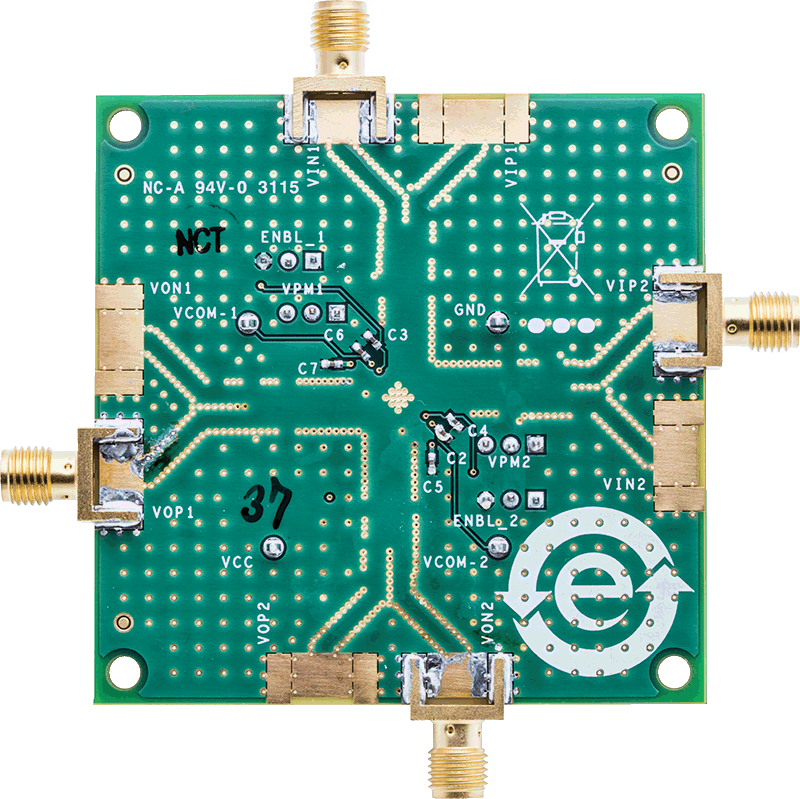
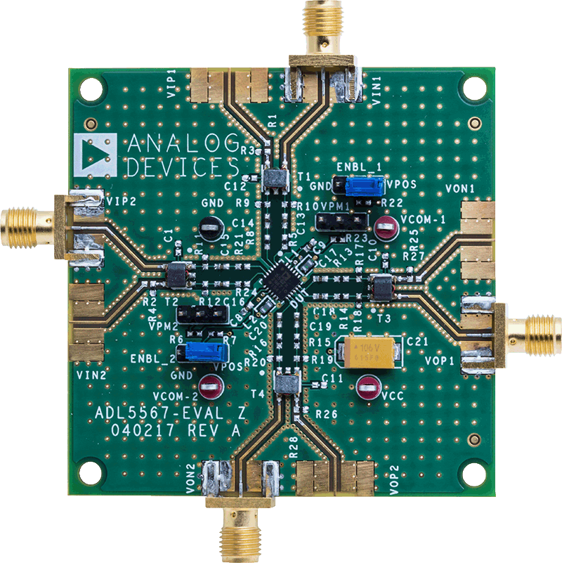
ADL5567 Evaluation Board