CN0304


Overview
Design Resources
Design & Integration File
- Schematic
- Bill of Materials
- Gerber Files
- PADS Files
- Assembly Drawing
Evaluation Hardware
Part Numbers with "Z" indicate RoHS Compliance. Boards checked are needed to evaluate this circuit.
- EVAL-CN0304-SDZ ($92.98) Low Power DDS Waveform Generator
- EVAL-SDP-CB1Z ($116.52) Eval Control Board
Device Drivers
Software such as C code and/or FPGA code, used to communicate with component's digital interface.
AD9834 - Microcontroller No-OS Driver
AD983x GitHub no-OS Driver Source Code
AD9834 IIO Direct Digital Synthesis GitHub Linux Driver Source Code
Features & Benefits
- 75MHz Low Power DDS
- Up to 18MHz Output
- 7th Order Elliptical Filter
Product Categories
Markets and Technologies
Parts Used
Documentation & Resources
-
CN-0304: Low Power DDS Waveform Generator2/26/2015PDF306 K
Circuit Function & Benefits
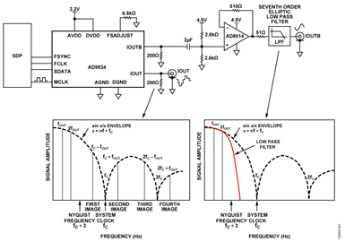
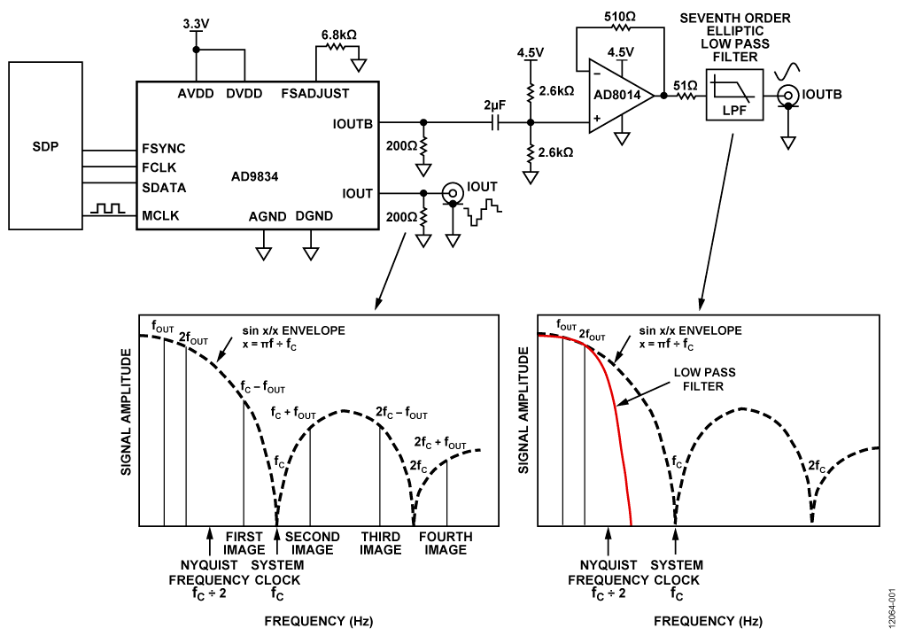
The circuit shown in Figure 1 is a 75 MHz low power (25 mW total) direct digital synthesis (DDS) waveform generator. The output buffer and anti-imaging filter provide improved spectral performance, making it suitable for frequency generation or clocking applications requiring sine wave, triangular wave, and square outputs up to 18 MHz.
Because they are sampled data devices, low power DDS devices must be followed by a suitable anti-imaging filter to remove spectral images. However, the maximum current output is approximately 4 mA into a recommended 200 Ω load; therefore, an optimum low power, low distortion op amp buffer at the DDS output provides a low impedance drive source for a high quality 50 Ω filter.
The combination of the DDS, output buffer, and seventh-order elliptic low pass filter provides high quality spectral performance.

Circuit Description
The AD9834 is a 75 MHz complete low power (20 mW) DDS. It is designed to provide true and complementary current outputs up to 4 mA with output frequencies up to 37.5 MHz.
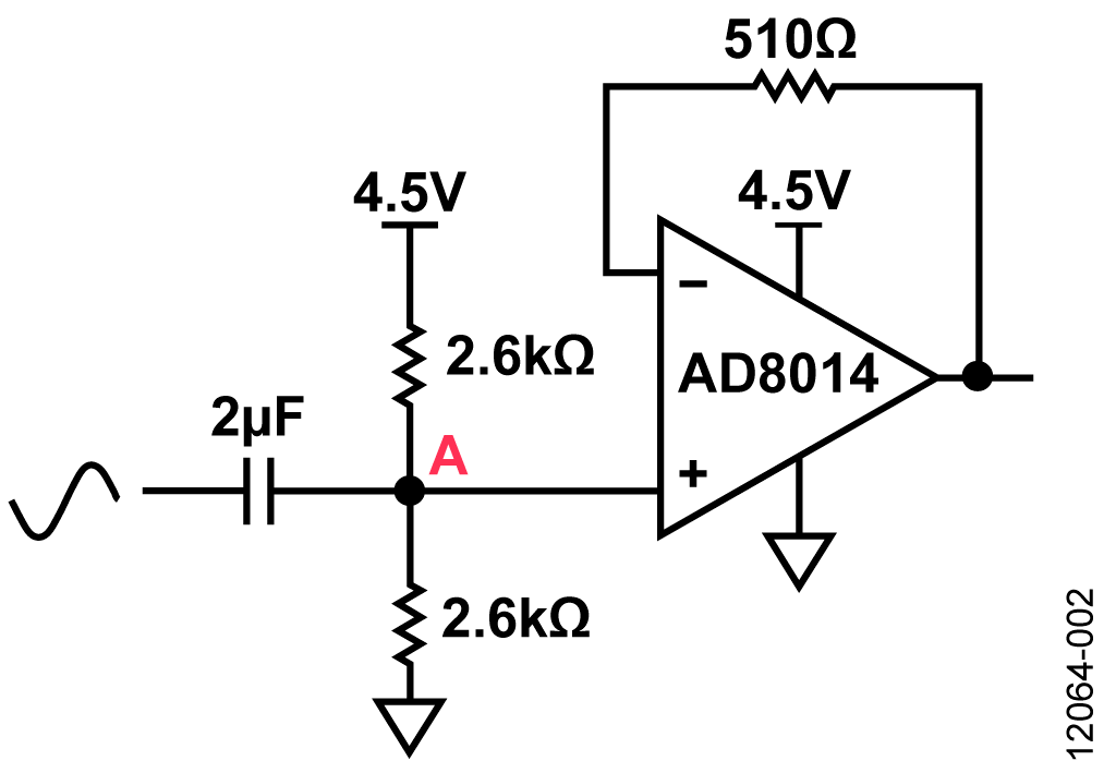
The AD8014 is a high speed current feedback amplifier with 400 MHz, −3 dB bandwidth, 4000 V/μs slew rate, and 24 ns settling time. It has extremely low voltage and current noise as well as low distortion. The low power (5.2 mW at +4.5 V), low cost, and 30 mA current drive capability make the AD8014 an attractive solution as a buffer for the AD9834 output. The circuit operates on +3.3 V for the AD9834 and +4.5 V for AD8014. The DDS operates with an SPI interface. The circuit consists of three blocks: the DDS block, the buffer block, and the low-pass filter block. Total power dissipation for the circuit is about 25 mW.
DDS Voltage Output
The full-scale adjust (FSADJUST) voltage and the external resistor, RSET, determine the magnitude of the full-scale DAC current. The FSADJUST has a nominal value of 1.15 V, while the RSET resistor has a typical value of 6.8 kΩ.
The full-scale current of the AD9834 is as follows:
IFULLSCALE = 18 × (FSADJUST/RSET)
This circuit uses a specified load of 200 Ω and maximum full-scale current to achieve voltage output without exceeding the compliance range of the DAC.
IFULLSCALE = 18 × (1.15/6800 Ω) = 3 mA,
VOUT = 3 mA × 200 Ω = 0.6 V
There are two current outputs available on the board: IOUT and IOUTB. The IOUT is unfiltered, and the IOUTB is filtered.
Buffer Amplifier
Due to the limited current and voltage compliance range at the output of the DDS, a buffer is necessary to provide higher current drive capability to the low-pass filter. In addition, the buffer provides isolation between the DDS block and the filter block and converts the 200 Ω output impedance of the loaded DDS to the 50 Ω required to drive the terminated filter. In this circuit note, the low-power high-performance current feedback operational amplifier AD8014 is used as an output buffer of the AD9834. The AD8014 is a high speed current feedback amplifier with 400 MHz, −3 dB bandwidth, 4000 V/μs slew rate and 24 ns settling time. It has an output current drive of ≥30 mA. The feedback resistor in the AD8014 current feedback op amp sets the bandwidth of the op amp.
Figure 2 shows the feedback resistor of 510 Ω. Because the op amp is operating from a single polarity supply, the output needs to be centered on mid-supply to prevent clipping. The voltage divider at point A provides a 2.25 V dc offset to the sinusoidal signal that gives an output swing of 2.25 V ± 0.3 V. For correct biasing of op amps in single supply applications, refer to Application Note AN-581, Biasing and Decoupling Op Amps in Single Supply Applications. For more information on current feedback amplifiers, refer to the MT-034 Tutorial, Current Feedback (CFB) Op Amps.

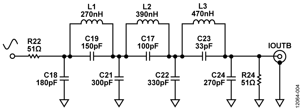
Seventh-Order Elliptic Low Pass Filter
The anti-imaging reconstruction must attenuate the image frequencies inherent to a sampled system as shown in Figure 1.
There are four basic filter types that can be used as a reconstruction filter: Cauer (elliptic), Chebyshev, Butterworth, and Bessel. Figure 3 shows the response curves of these four basic filter types.


For the same order, the elliptic filter has a higher roll-off rate compared to the other three, therefore, it makes an attractive candidate for the reconstruction filter. The filter used in this circuit note is a 7th order elliptic filter with a −3 dB bandwidth of 18 MHz.
Component Selection
The resistors, capacitors, and inductors used to implement the filter are passive components, and, due to the high frequencies involved, must meet the following requirements:
- Low parasitic capacitance and inductance.
- Low tolerance values so that the measured response is close to the design response.
- Wide temperature range.
- Small physical to minimize parasitic capacitance and inductance.
These are just a few of the criteria that ensure measured filter response is close to the simulated filter response.
For more information on selecting passive components for specific application, please refer to Basic Linear Design: Chapter 10, Passive Components.
Filter Design and Performance
The 7th order elliptic filter is shown in Figure 4, and the simulated and actual frequency response of the filter is shown in Figure 5. The software used is Advances Design System (ADS) Version 2012.08. The actual filter components and manufacturers can be found in the bill-of-materials in the CN0304 Design Support Package at http://www.analog.com/CN0304-DesignSupport.


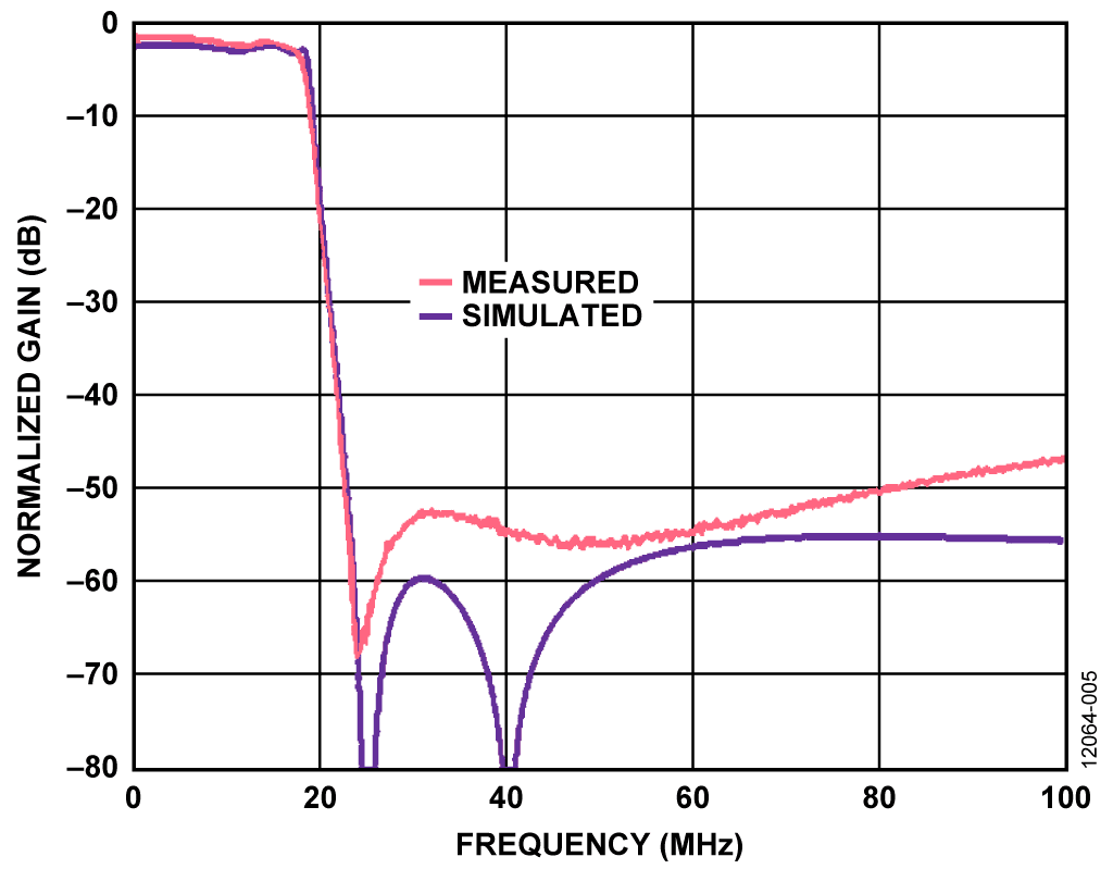
The measured filter response was taken using the Agilent E5061B Network Analyzer. It shows the −3 dB bandwidth to be 18 MHz. The pass band attenuation is approximately 6 dB due to the source and load termination.
To check the performance of the circuit, the spectrum of the DDS output were measured with AD9834 set to an output frequency of 15 MHz with a 75 MSPS clock. The unfiltered and filtered outputs are shown in Figure 6 and Figure 7, respectively.
As shown in Figure 7, there is a significant reduction of the undesired images that appear in the unfiltered spectrum of Figure 6. The highest image spur at 60 MHz is suppressed by about 52 dB relative to the unfiltered output. This corresponds to the measured attenuation of the filter at 60 MHz.

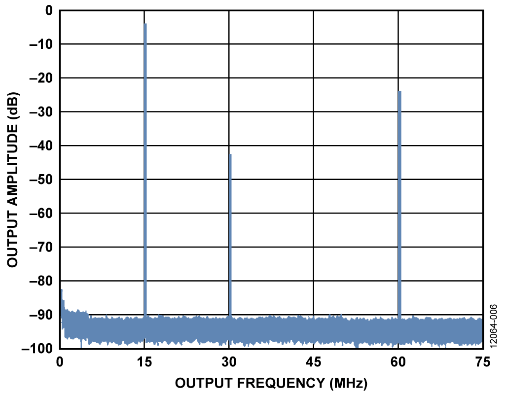


The 600 mV p-p output of the AD9834 is attenuated by approximately 6 dB by the filter, and an additional 1 dB by the sin x/x roll off. The output into the 50 Ω load is therefore approximately 268 mV p-p, or 94.7 mV rms. This corresponds to 0.179 mW, or −7.5 dBm.
For more information on the reconstruction filter design for DDS, refer to Application Note AN-837, DDS-Based Clock Jitter Performance vs. DAC Reconstruction Filter Performance.
The circuit must be constructed on a multilayer PC board with a large area ground plane. Proper layout, grounding, and decoupling techniques must be used to achieve optimum performance (see MT-031 Tutorial, Grounding Data Converters and Solving the Mystery of “AGND” and “DGND,” and MT-101 Tutorial, Decoupling Techniques).
Complete design support package including schematics, layouts, and bill of materials can be found at http://www.analog.com/CN0304-DesignSupport.
Common Variations
An alternative for the DDS is the AD9838. It has lower power (11 mW) and offers the same functionality of the AD9834 but with lower clock rate of 16 MHz.
The buffer used in this circuit note is the current-feedback amplifier AD8014. An alternative for this is the ADA4860-1. It is a low cost, high speed (800 MHz, −3 dB bandwidth), low power (22.5 mW at 5 V), current feedback operational amplifier, but with a lower slew rate of 790 V/μs.
Another alternative is the ADA4897-1. It is a unity-gain stable, low wideband noise, rail-to-rail output high speed voltage feedback amplifier, with input voltage noise of 2.4 nV/√Hz at 10 Hz and a spurious free dynamic range (SFDR) of −80 dBc at 2 MHz.
The ADA4851-1 can also be used as buffer. It is a low cost, low power, high-speed (−3 dB bandwidth of 130 MHz) device, but with much a lower slew rate of 375 V/μs.
Circuit Evaluation & Test
Equipment Required
- EVAL-CN0304-SDZ evaluation board
- EVAL-SDP-CB1Z evaluation board
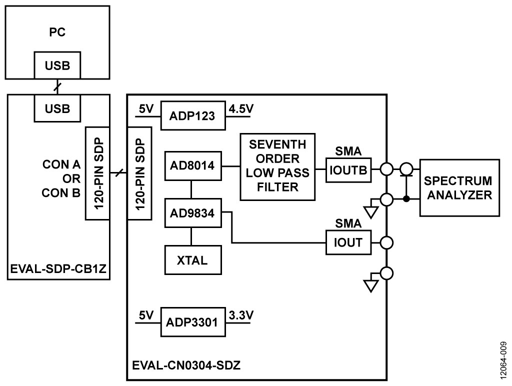
- AD9834 Evaluation Software
- Agilent E3631A triple output dc power supply or equivalent
- Rohde and Schwarz FSUP50 Signal Source Analyzer
- Agilent E5061B Network Analyzer (needed only to evaluate the filter response)
Filter Response Measurement
The frequency response of the filter was measured with a network analyzer using the setup shown in Figure 8.

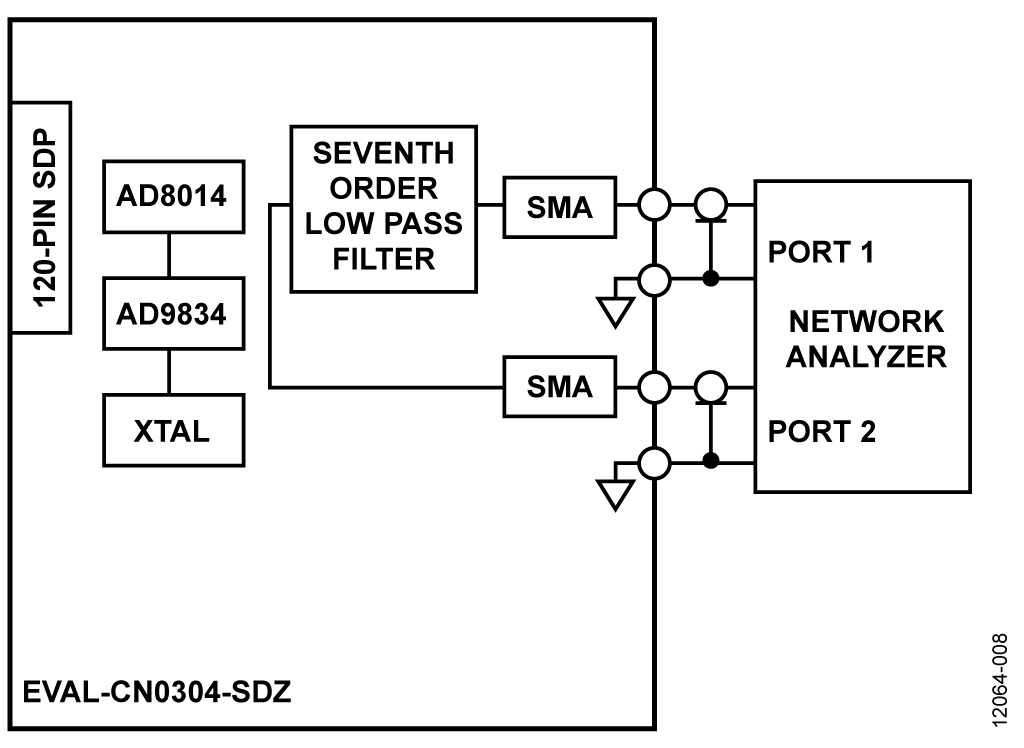
The EVAL-CN0304-SDZ board was modified, and the signal from the network analyzer applied to the input of the filter. The output of the filter was connected to the second port of the analyzer.

The 5 V supply for the EVAL-CN0304-SDZ is derived from the 5 V USB voltage from the SDP card. Set the jumpers as follows: LK1 in B position, LK2 in B position, and LK3 removed.
The AD9834 Evaluation Software, located at ftp://ftp.analog.com/pub/evalcd/AD9834/, was used to set the output frequency and amplitude of the DDS. See the AD9834 Evaluation Board User Guide, UG-266 for further details. The hardware described in UG-266 does not have the 7th order output filter; however, the graphical user interface and software operation is identical to the EVAL-CN0304-SDZ hardware.
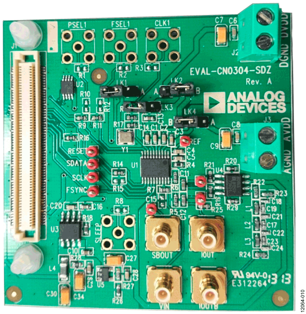
A photograph of the CN0304 printed circuit board is shown in Figure 10.