AN-2046: IEC 61000-4-x & CISPR 11 Tested Analog Output Design with the AD5758 & ADP1031 for Ind. Process Control Apps
AN-2046: IEC 61000-4-x and CISPR 11 Tested Analog Output Design with the AD5758 and ADP1031 for Industrial Process Control Applications
INTRODUCTION
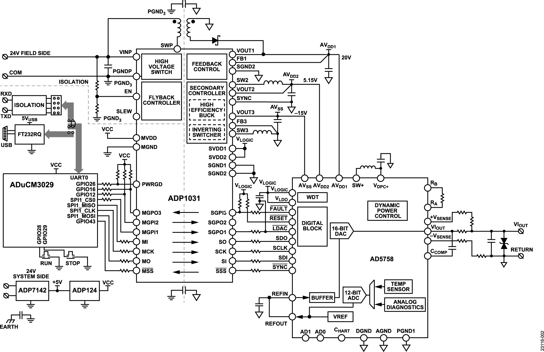
The AD5758 is a single-channel, 16-bit, voltage and current output digital-to-analog converter (DAC) with on-chip dynamic power control (DPC) and HART® connectivity. The AD5758 is designed to work with programmable logic controller (PLC) and distributed control system (DCS) modules of industrial process control applications.
The ADP1031 is a high performance, isolated micropower management unit (microPMU) that provides three isolated power rails. Additionally, the ADP1031 contains four high speed serial peripheral interface (SPI) isolation channels and three general-purpose isolators for channel to channel applications where low power dissipation and small solution size are required.
This application note describes an electromagnetic compatibility (EMC) tested solution of the analog output design with the ADP1031ACPZ-1-R7 (hereafter referred to as the ADP1031) and the AD5758 output voltage (VOUT) and output current (IOUT) for industrial process control with dynamic power control. The IEC 61000-4-x set of standards cover the evaluation of the immunity of electrical and electronic equipment at a system level.
The AD5758 and ADP1031 EMC test board is characterized to ensure that the circuit performance is not affected by radiated RF or conducted RF disturbances, and has sufficient immunity against electrostatic discharge (ESD), electrical fast transients (EFT), and surge. The EMC test board was also tested per the CISPR 11 standard, in which the radiated emissions of the board are well below the Class B limits due to the improved electromagnetic interference (EMI) performance of the ADP1031. The ADP1031 passes the CISPR 11 Class B limits with a greater than 9 dB margin, due to its high integration and design optimizations. The AD5758 and ADP1031 EMC test board design significantly reduces the risk of failing IEC 61000-4-x and CISPR 11 certification in multichannel analog output applications with the AD5758 and ADP1031.
The AN-1599 Application Note, IEC 61000-4-x and CISPR 11 Tested Analog Output Design with the AD5758 for Industrial Process Control Applications, describes the AD5758 EMC test board, which shares the same blank PCB of this board but is assembled with partially different bill of materials (BOM). The AD5758 EMC test board uses discrete ICs to implement the power and digital isolation of the ADP1031. The AD5758 EMC test board has comparable immunity but only passes CISPR 11 Class A limits. Refer to the AN-1599 Application Note for additional details.


SYSTEM DESIGN
AD5758 DAC DESCRIPTION
The AD5758 is a single-channel, voltage and current output DAC that operates with a 60 V maximum operating voltage between the AVSS and AVDD1 rails. The on-chip DPC minimizes package power dissipation, which is achieved by regulating the supply voltage (VDPC+) to the VIOUT output driver circuitry from 5 V to 27 V using a buck dc-to-dc converter. The CHART pin enables a HART signal to couple to the current output.
The device uses a versatile, 4-wire serial peripheral interface (SPI) that operates at clock rates of up to 50 MHz and is compatible with standard SPI, QSPI™, MICROWIRE™, DSP, and microcontroller interface standards. The interface also features an optional SPI cyclic redundancy check (CRC) and a watchdog timer (WDT). The AD5758 offers diagnostic features, such as output current monitoring and an integrated 12-bit diagnostic analog-to-digital converter (ADC). Additional robustness is provided by the inclusion of a fault protection switch on the VIOUT, +VSENSE, and −VSENSE pins.
For full details, refer to the AD5758 data sheet.
ADP1031 MICROPOWER MANAGEMENT UNIT DESCRIPTION
The ADP1031 is a high performance, isolated microPMU that combines an isolated flyback dc-to-dc regulator, an inverting dc-to-dc regulator, and a buck dc-to-dc regulator, providing three isolated power rails.
CIRCUIT DESCRIPTION
This circuit is a single-channel, isolated, industrial voltage and current output module for harsh EMI/EMC environments featuring the AD5758 DAC and ADP1031 microPMU with seven digital isolators. This design is targeted for PLC and DCS applications. The AD5758 and ADP1031 EMC test board is designed to satisfy the IEC 6100-4-x and CISPR 11 standards intended for use in the harsh industrial environments that is stated in IEC 61000-6-2 generic standard. The AD5758 and ADP1031 EMC test board is a BOM variant of the AD5758 EMC test board described in the AN-1599. These two boards are assembled on the same blank PCB. The only difference of the variant in this application note is that the ADP1031 replaces the discrete power and digital isolation implementation consisting of the LT8300, ADP2360, ADuM141D, ADuM142D, and ADM6339.
Powering the Design
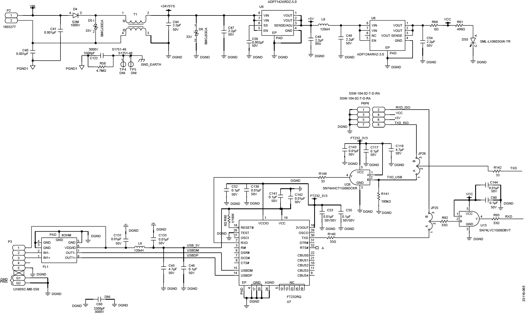
The AD5758 and ADP1031 EMC test board is powered by two separate supplies. The first 24 V input is supplied to the ADP1031, which greatly simplifies the isolated power supply design. On this EMC test board, the ADP1031 is used to generate an isolated 20 V and powers the AVDD1 pin of the AD5758. The ADP1031 5.15 V VOUT2 and −15 V VOUT3 also supply the voltage for the AVDD2 and AVSS pins of the AD5758, respectively. The second 24 V supply powers the circuits on the system side domain, including the microprocessor and digital isolator. The ADP7142 steps the 24 V supply down to 5 V, which supplies the circuits where 5 V logic or 5 V power is required. A low dropout (LDO) regulator, the ADP124, further regulates the 5 V supply to 3 V for low power components, including the ADuCM3029. The AD5758 and ADP1031 EMC test board can operate from a single 24 V supply, but the two 24 V supplies must be isolated from each other to demonstrate that the system power and the field power are separate power supplies. The two 24 V supplies are meant to mimic the typical use case, where the system power and the field power are supplied separately within the system.
Isolation Considerations
A properly placed isolation barrier is often the first method used to improve EMC robustness. The ADP1031 provides electrical isolation between the field side AD5758 and the system side microcontroller unit (MCU). Take precautions to achieve optimal EMC and EMI performance. For optimum radiated emission performance, it is recommended to connect an inductor and capacitor (LC) filter, consisting of a ferrite bead and 100 nF and 10 nF capacitors in parallel to each other, to the MVDD, SVDD1, and SVDD2 pins. A 0.001 μF ceramic capacitor across the isolation barrier also reduces the radiated emission. See the AN-1109 Application Note, Recommendations for Control of Radiated Emissions with iCoupler Devices, for more details.
The ADP1031 isolated flyback converter drives a flyback transformer. A 1 nF, 3 kV capacitor across the primary and secondary side provides a return path for the image current.
The ADuCM3029 ultra low power Arm® Cortex®-M3 MCU provides local control and data communication for the AD5758 and ADP1031 EMC test board. The ADuCM3029 has an acceptable emission profile and has adequate immunity in the IEC 61000-4-x tests.

PRINTED CIRCUIT BOARD
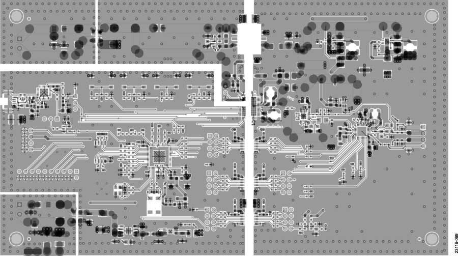
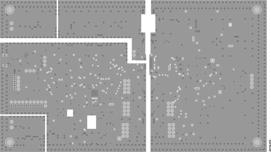
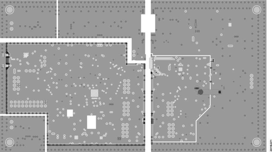
The AD5758 and ADP1031 EMC test board is built on a FR4 4-layer printed circuit board (PCB). The primary side and the secondary side of the PCB have 0.5 oz copper foil, and the internal layers are on 1 oz copper. The PCB stack is illustrated in Figure 3.


COMPONENT PLACEMENT AND LAYOUT CONSIDERATIONS
This section describes design considerations for optimal EMC and EMI performance of the AD5758 with the minimum man-datory components (general recommendations on component placement, and distances from connector).
Place the digital interface side of the AD5758 close to the isolators. The damping resistors (around a few tens of ohms to hundreds of ohms) on the digital lines attenuate the electrical transients due to the CMOS switching on and off, which helps to reduce EMI. The VIOUT side of the AD5758 must be close to the 4-pin output terminal block on the edge of the AD5758 and ADP1031 EMC test board.
Other Component Considerations
The AD5758 and ADP1031 EMC test board uses 0.1 μF, 50 V, X7R, 10%, low equivalent series resistance (ESR) ceramic capacitors in the C0603 footprint for the decoupling capacitors, which is a trade-off among considerations for performance, derating, cost, and space savings. In some cases, when closer decoupling is required, a 1 nF, 25 V, X7R capacitor in the C0402 footprint is applied.
Voltage Supply Protection
The scope of EMC or EMI evaluation and demonstration focuses on the AD5758 and its companion parts. The two 24 V power supply circuits on the AD5758 and ADP1031 EMC test board provide the necessary voltages for the function of the board. The supply circuits are not intended to match the robustness of the power supply module or the backplane supply in the automation control system of a user. Therefore, only basic protections are implemented for these supply circuits. In the 24 V supply for the system side, a 1 nF capacitor is placed next to each pin of the power input terminal to the protected ground, where transient energy can be discharged to the earth ground through a 3.3 nF, 3 kV capacitor. The 4.7 MΩ resistor bleeds energy to the earth, which can accumulate on the protected ground. A transient voltage suppression (TVS) diode is inserted to prevent miswiring to the power supply input. The TVS diode clamps the transient voltage from going higher than 33 V (nominal). A common-mode inductor attenuates the emissions escaping from the downstream circuits. A second TVS diode is inserted after the inductor provides further clamping for the transient. The 24 V power supply for the field side has a similar protection scheme.
ESD Protection
The AD5758 and ADP1031 EMC test board must have appropriate ESD protection circuitry. The protection consists of a current limiting resistor, a transient voltage clamp, and a transient energy diverting capacitor.
There are three minimum mandatory components for EMC and EMI of the AD5758. A 10 Ω resistor on the trace between the AD5758 VIOUT pin and the terminal block limits the transient current to and from the device. The TVS diode is crucial to clamp the electrical transient on the board during EMC events. A TVS diode is inserted between the AD5758 and the output terminal block. The pins of the TVS diode are directly routed to the VIOUT and RETURN screws (on the P4 terminal) with short and heavy traces. A 10 nF, 50 V, X7R capacitor located in parallel to the TVS diode diverts the small amount of high frequency transient to the RETURN screw. Optional clamp diodes connected to the AVDD1 and AVSS rails can be added to the VIOUT line to further improve the robustness. However, these diodes are unnecessary for the AD5758 and ADP1031 EMC test board because the EMC and EMI performance objectives are met without them.


CIRCUIT EVALUATION AND TEST
The AD5758 reference design is run by being connected to a PC or run in standalone mode. The graphic user interface (GUI) on the PC configures the running parameters, such as DAC output range, output code, and ADC sequencing. The GUI displays the fault flag map and plots the reading from the AD5758 on-chip, diagnostic ADC nodes.
When the operational parameters are programmed in the on-board flash memory, the board can be disconnected from the PC or controller board when the software is operating. To operate the board, power up the board and press the RUN or STOP buttons on the AD5758 and ADP1031 EMC test board.
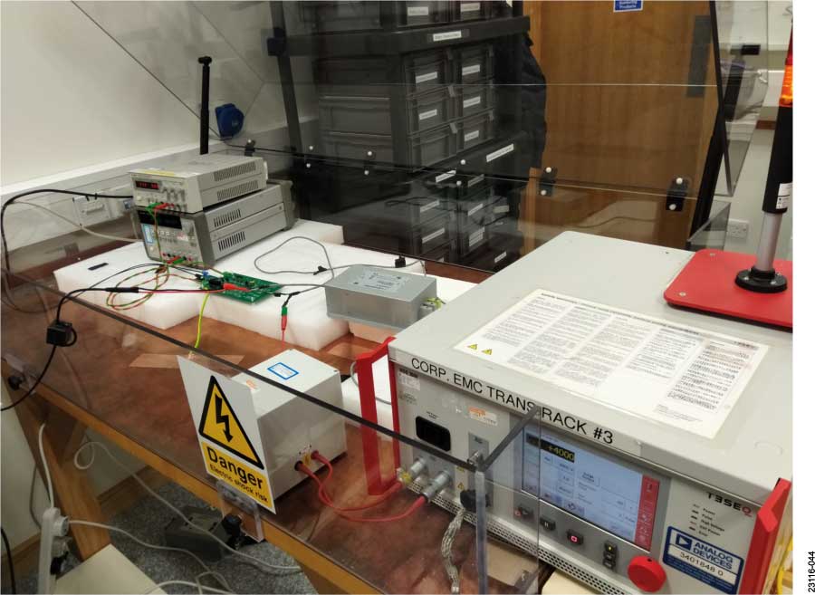
Figure 5 shows the general setup of the AD5758 and ADP1031 EMC test board for EMC tests. Before and after each potentially destructive EMC test, the precision bench digital multimeter (DMM) takes 300 measurements of the AD5758 output on the load resistor. The deviation between the two sets of DMM measurements must stay within the predefined range to meet the performance criterion. The maximum allowable deviation is 0.1% of full scale, which aligns with the common requirements of the industrial automation applications.
During the nondestructive EMC tests, the bench DMM contin-uously measures the AD5758 output on the load resistor. The measurements taken during and after the EMC event are compared to the average of the DMM measurement before the EMC event for judging the performance criterion.
In the emissions test, the AD5758 is configured to output the full-scale voltage or current that is being refreshed at 1 kHz, and the AD5758 and ADP1031 EMC test board runs in standalone mode. The only auxiliary devices in this setup are two 24 V battery packs that power the AD5758 and ADP1031 EMC test board. These battery packs are assumed to not contribute EMI.
SOFTWARE NEEDED
To perform EMC testing on the AD5758, the following software is required:
- Firmware, Revision 57-58-E0-01 on the AD5758 and ADP1031 EMC test board
- AD5758 system EMC GUI software, Revision 1.0.0.1
- Keysight Technologies BenchVue™ software, Version 2.6
EQUIPMENT NEEDED
To perform EMC testing on the AD5758, the following equipment is required:
- Optical USB transceiver board
- Industrial fiber optic cable
- PC running Windows® 7, 64-bit version, image model: V3.0.2011.10.14
- DC power supplies: Agilent 3630A and Agilent 3631A
- Digital multimeter: Keysight 33470A
- 2 m (1 pair twisted) conductor multiconductor cable: Belden 8761
- Line filter: Schaffner FN353Z-30-33
A load resistor is connected to the AD5758 by a 2 m cable (Belden 8761, twisted, shielded pair). In current output mode, the load is a radial leaded, 500 Ω, ±0.005%, ±0.8 ppm/°C, 600 mW, 300 V foil resistor. In voltage output mode, the load is a radial leaded, 1 kΩ, ±0.01%, ±0.8 ppm/°C, 600 mW, 300 V foil resistor.
A pair of twisted leads, followed by a low-pass filter, probes the voltage across the load resistor. The filter output is wired to the Keysight 33470A DMM with a pair of twisted leads. The DMM integration time is set to a 0.02 power line cycle (400 μs). A USB cable connects the DMM to the PC. The AD5758 GUI software monitors the AD5758 status register every 1 ms via the electrically isolated data link.
The AD5758 system EMC GUI software sends parameters to the local microprocessor to write to the AD5758. For each EMC and EMI test item, the AD5758 and ADP1031 EMC test board is tested in voltage output mode and current output mode.
Two output conditions are checked in each output mode. The first condition is an alternated write of 0xFFFF and 0x8000 to the AD5758 every 2 sec to verify that the AD5758 output is actively updated according to the input code during the EMC tests. The second condition is a fixed write of 0xFFFF to the AD5758 every 1 ms for the simplified calculation of the AD5758 output deviation, during and after EMC events.


The AD5758 and ADP1031 EMC test board is tested to and meets the CISPR 11 and IEC 61000-4-x standards described in Table 1 and Table 2. Table 3 describes the performance criteria listed in Table 2.
STANDARDS AND PERFORMANCE CRITERIA
The AD5758 and ADP1031 EMC test board is designed to pass the EMC and EMI test items and limits, and to meet the performance criteria. The EMC test board limits and performance criteria are defined according to the IEC 61000-6-2 and the IEC 61131-2 standards. According to these standards, the following six applicable tests were selected:
- IEC 61000-4-2
- IEC 61000-4-3
- IEC 61000-4-4
- IEC 61000-4-5
- IEC 61000-4-6
- CISPR 11
| Test | Basic Standard | Frequency Range (MHz) | Limits | Measured Minimum Margin (dBμV/m) | Result |
| Radiated Emissions | CISPR 11, Class B | 30 to 1000 | See Table 11 and Table 12 | 9.07 | Pass |
| Test | Basic Standard | Test Levels | Performance Criterion | Measured Minimum Margin |
Result |
| Conducted Immunity | IEC 61000-4-6 | 20 V/m | A | See Table 4 | Pass |
| Radiated Immunity | IEC 61000-4-3 | 20 V/m | A | See Table 10 | Pass |
| ESD | IEC 61000-4-2 IEC 61000-4-2 IEC 61000-4-2 |
±6 kV contact ±12 kV air ±30 kV coupling |
B B B |
See Table 5 See Table 6 See Table 7 |
Pass Pass Pass |
| EFT | IEC 61000-4-4 | ±4 kV | B | See Table 8 | Pass |
| Surge | IEC 61000-4-5 | ±4 kV | B | See Table 9 | Pass |
| Performance Criterion | Description |
| A | Normal performance within an error band specified by the manufacturer. |
| B | Temporary loss of function or degradation of performance, which ceases after the disturbance is removed. The equipment under test (EUT) recovers its normal performance without operator intervention. |
| C | Temporary loss of function or degradation of performance. Correction of performance requires operator intervention, such as manual restart, power off, or power on. |
| D | Loss of function or degradation of performance, which is not recoverable. Permanent damage to hardware or software, or loss of data. |
EMC AND EMI MEASUREMENT RESULTS OF THE AD5758 AND ADP1031 EMC TEST BOARD
CONDUCTED IMMUNITY
As per IEC 61000-4-6, the EUT is placed on an insulating support that is 0.1 m high above a ground reference plane. All cables exiting the EUT are supported at a height of at least 30 mm above the ground reference plane. The interference is injected with a coupling and decoupling network (CDN), 801A. The cable is decoupled by an attenuation clamp, KEMZ 801A. The frequency range is swept from 150 kHz to 80 MHz (20 V/m) with the disturbance signal of 80% amplitude modulated with a 1 kHz sine wave. The step size is 1% of the start and thereafter 1% of the preceding frequency value where the frequency is swept incrementally. The dwell time of the amplitude-modulated carrier at each frequency is 0.5 sec. During this interval, the DMM is able to complete more than 30 measurements, which is adequate for calculating the error deviation.
| Output Mode | Average Before Zap | During Zap | Average After Zap | Deviation of Full Scale (ppm) | Pass or Fail | |
| Minimum | Maximum | |||||
| VOUT = 10 V | 9.999341 V | 9.997904 V | 10.000008 V | 9.999395 V | −0.009%, 0.004% | Pass, Criterion A |
| IOUT = 20 mA | 19.960074 mA | 19.959014 mA | 19.962312 mA | 19.960025 mA | −0.007%, 0.014% | Pass, Criterion A |


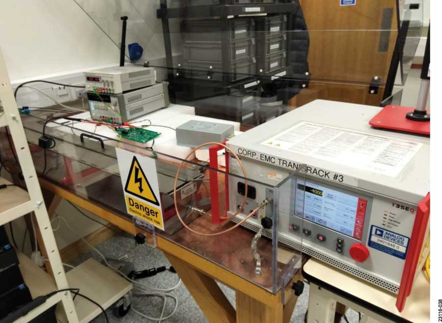
IMMUNITY TO ESD
The test setup consists of a nonconductive table with a height of 0.8 m, standing on the ground reference plane. A 1.6 m × 0.8 m horizontal coupling plane (HCP) is placed on the table. The EUT and its cable are isolated from the coupling plane by an insulating mat that is 0.5 mm thick.
The contact discharges are applied to the VIOUT and RETURN terminal screws of the AD5758 output terminal block (P4). The EUT is exposed to at least 20 discharges at each rating, 10 each at negative and positive polarity. The discharges are repeated at a rate of one discharge per second.
The air discharges are applied to the AD5758 output terminal block. The EUT is exposed to at least 20 discharges at each rating: 10 each at negative and positive polarity. The discharges are repeated at a rate of one discharge per second.
The coupling discharge are applied to the HCP and vertical coupling plane (VCP). The EUT is exposed to at least 20 discharges at each rating: 10 each at negative and positive polarity. The discharges are repeated at a rate of one discharge per second. The coupling plane has two 470 kΩ bleeding resistors to earth ground.
| Test Level | Output Mode | Zap Point on P4 | Before Zap | After Zap | Deviation of Full Scale (ppm) | Pass or Fail |
| 6 kV Contact Discharge | VOUT = 10 V | VIOUT terminal screw | 9.999939 V | 9.999964 V | 3 | Pass, Criterion B |
| VOUT = 10 V | RETURN terminal screw | 9.999946 V | 9.999965 V | 2 | Pass, Criterion B | |
| IOUT = 20 mA | VIOUT terminal screw | 19.961543 mA | 19.961512 mA | −2 | Pass, Criterion B | |
| IOUT = 20 mA | RETURN terminal screw | 19.961495 mA | 19.961551 mA | 3 | Pass, Criterion B | |
| −6 kV Contact Discharge | VOUT = 10 V | VIOUT terminal screw | 9.998116 V | 9.998157 V | 4 | Pass, Criterion B |
| VOUT = 10 V | RETURN terminal screw | 9.999761 V | 9.999805 V | 5 | Pass, Criterion B | |
| IOUT = 20 mA | VIOUT terminal screw | 19.961541 mA | 19.961490 mA | −3 | Pass, Criterion B | |
| IOUT = 20 mA | RETURN terminal screw | 19.961426 mA | 19.961442 mA | 1 | Pass, Criterion B |
| Test Level | Output Mode | Zap Point on P4 | Before Zap | After Zap | Deviation of Full Scale (ppm) | Pass or Fail |
| 12 kV Air Discharge | VOUT = 10 V | VIOUT terminal block | 9.999615 V | 9.999612 V | −1 | Pass, Criterion B |
| IOUT = 20 mA | VIOUT terminal block | 19.960970 mA | 19.960972 mA | 1 | Pass, Criterion B | |
| −12 kV Air Discharge | VOUT = 10 V | VIOUT terminal block | 9.999562 V | 9.999572 V | 1 | Pass, Criterion B |
| IOUT = 20 mA | VIOUT terminal block | 19.960957 mA | 19.961000 mA | 2 | Pass, Criterion B |
| Test Level | Output Mode | Zap Point | Before Zap | After Zap | Deviation of Full Scale (ppm) | Pass or Fail |
| 30 kV Coupling Discharge | VOUT = 10 V | Horizontal plane | 10.000360 V | 10.000379 V | 2 | Pass, Criterion B |
| VOUT = 10 V | Vertical plane | 10.000385 V | 10.000371 V | −2 | Pass, Criterion B | |
| IOUT = 20 mA | Horizontal plane | 19.961024 mA | 19.960967 mA | −3 | Pass, Criterion B | |
| IOUT = 20 mA | Vertical plane | 19.961045 mA | 19.960978 mA | −4 | Pass, Criterion B | |
| −30 kV Coupling Discharge | VOUT = 10 V | Horizontal plane | 10.000398 V | 10.000384 V | -2 | Pass, Criterion B |
| VOUT = 10 V | Vertical plane | 10.000387 V | 10.000378 V | −1 | Pass, Criterion B | |
| IOUT = 20 mA | Horizontal plane | 19.961049 mA | 19.961004 mA | −3 | Pass, Criterion B | |
| IOUT = 20 mA | Vertical plane | 19.961010 mA | 19.960995 mA | −1 | Pass, Criterion B |


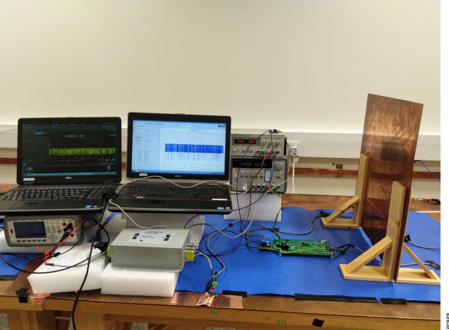


IMMUNITY TO ELECTRICAL FAST TRANSIENTS
Per the IEC 61000-4-4 standard, the EUT is tested with 4000 V discharges on the analog input cable. Positive and negative polarity discharges are applied. The length of the hot wire from the coaxial output of the EFT generator to the terminals on the EUT must not exceed 1 m. The duration time of each test sequential is 1 min. The transient and burst waveform is in accordance with IEC 61000-4-4, 5 ns rising time with 50 ns pulse width.
The configuration consists of a 0.8 m high wooden table, covered with a sheet of copper that is at least 0.25 mm thick, and connected to the protective grounding system. The EUT is placed on a 0.1 m thick isolating support. A minimum distance of 0.5 m is provided between the EUT and the walls of the laboratory.
| Test Level | Output Mode | Before Zap | After Zap | Deviation of Full Scale (ppm) |
Pass or Fail |
| 4 kV EFT | VOUT = 10 V | 10.000216 V | 10.000277 V | 4 | Pass, Criterion B |
| IOUT = 20 mA | 19.960184 mA | 19.960118 mA | −5 | Pass, Criterion B | |
| −4 kV EFT | VOUT = 10 V | 10.000269 V | 10.000254 V | −1 | Pass, Criterion B |
| IOUT = 20 mA | 19.960140 mA | 19.960190 mA | 4 | Pass, Criterion B |


IMMUNITY TO SURGE
Per the IEC 61000-4-5 standard for industrial environments, the surge is a combination wave of 1.2 μs rising time with 50 μs pulse width open circuit voltage and 8 μs rising time with 20 μs pulse width short-circuit current. The EUT is subject to five positive and five negative surges at each rating. The interval between each surge is 1 min. The surge is tested to the AD5758 output cable, which is treated as unshielded asymmetrically operated interconnection lines of the EUT. The surge is applied to the lines via capacitive coupling through CDN 174.
The CDNs do not influence the specified functional conditions of the EUT. The interconnection line between the EUT and the CDNs is 2 m in length or shorter.
| Test Level | Output Mode | Before Zap | After Zap | Deviation of Full Scale (ppm) |
Pass or Fail |
| 4 kV Surge | VOUT = 10 V | 9.999588 V | 9.999406 V | −12 | Pass, Criterion B |
| IOUT = 20 mA | 19.960027 mA | 19.960030 mA | 1 | Pass, Criterion B | |
| −4 kV Surge | VOUT = 10 V | 9.999328 V | 9.999389 V | 4 | Pass, Criterion B |
| IOUT = 20 mA | 19.959943 mA | 19.959980 mA | 3 | Pass, Criterion B |


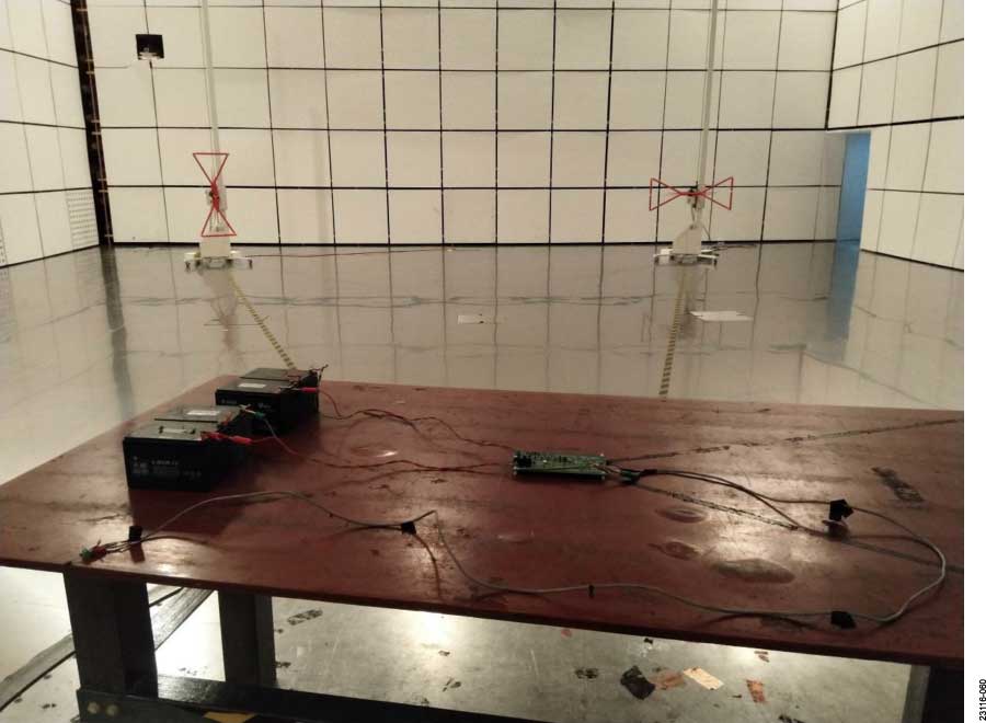
RADIATED IMMUNITY
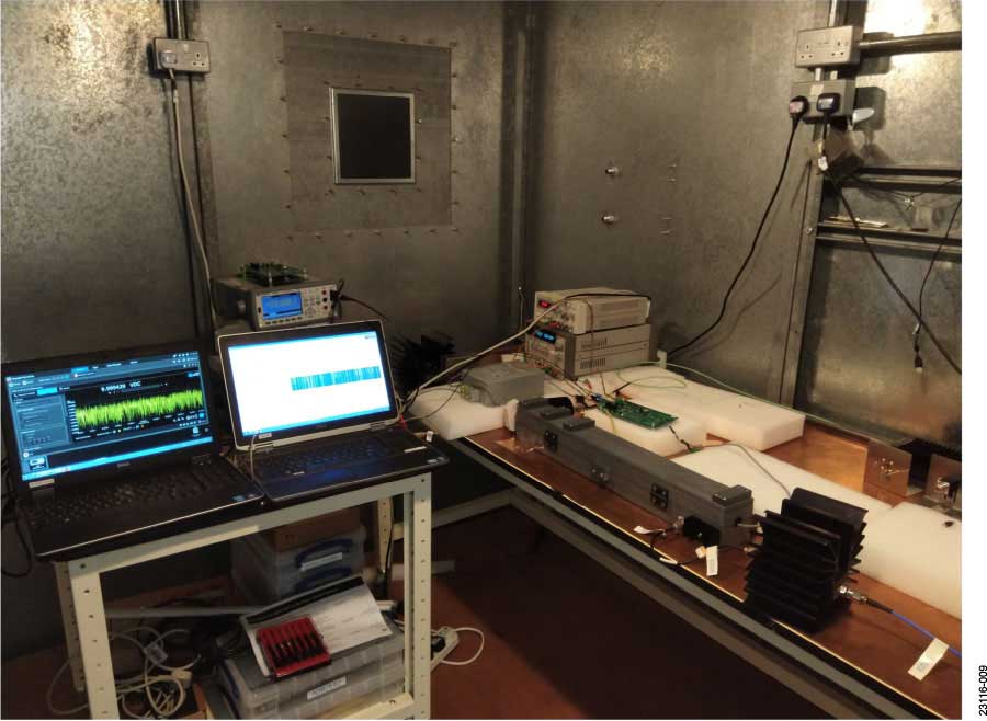
Per the IEC 61000-4-3 standard for industrial environments, the test is performed in a fully anechoic chamber. The EUT is placed on a 0.8 m high nonconductive table. A DMM, used as auxiliary equipment, is put in a shielded box under the table and probes the AD5758 output at the load resistor. The DMM measurement data is sent to the PC outside the chamber via an Ethernet cable. The transmit antenna is located 3 m from the EUT. The frequency range is swept from 80 MHz to 1000 MHz, and from 1000 MHz to 6000 MHz with the 80% signal amplitude modulated with a 1 kHz sine wave. The frequency range is swept incrementally, and the step size is 1% of the preceding frequency value. The dwell time at each frequency is 1 sec, which is not less than the time necessary for the EUT to respond. During this interval, the DMM is able to complete 20 measurements, which is adequate for calculating the error deviation. The field strength is 20 V/m in the 80 MHz to 1000 MHz range. The field strength for the 1000 MHz to 6000 MHz range is 10 V/m. The test is performed with the EUT exposed to a vertically and horizontally polarized field.
| Frequency Range | Test Level | Antenna Polarization | Output Mode | Average | During Zap (Maximum) | During Zap (Minimum) | Deviation 0f Full Scale (%) | Pass or Fail |
| 80 MHz to 1000 MHz | 20 V/m | Horizontal | VOUT = 10 V | 9.999848 | 10.000866 | 9.998624 | −0.013, 0.010 | Pass, Criterion A |
| 20 V/m | Vertical | VOUT = 10 V | 9.999883 | 10.001688 | 9.998599 | −0.012, 0.019 | Pass, Criterion A | |
| 20 V/m | Horizontal | IOUT = 20 mA | 19.996675 | 19.998610 | 19.994331 | −0.012, 0.009 | Pass, Criterion A | |
| 20 V/m | Vertical | IOUT = 20 mA | 19.996793 | 20.000425 | 19.994738 | −0.011, 0.018 | Pass, Criterion A | |
| 1000 MHz to 6000 MHz | 10 V/m | Horizontal | VOUT = 10 V | 9.999852 | 10.000866 | 9.998709 | −0.011, 0.010 | Pass, Criterion A |
| 10 V/m | Vertical | VOUT = 10 V | 9.999827 | 10.000857 | 9.998649 | −0.012, 0.010 | Pass, Criterion A | |
| 10 V/m | Horizontal | IOUT = 20 mA | 19.996832 | 19.998542 | 19.994976 | −0.010 0.008 | Pass, Criterion A | |
| 10 V/m | Vertical | IOUT = 20 mA | 19.996822 | 19.998695 | 19.994976 | −0.009, 0.010 | Pass, Criterion A |


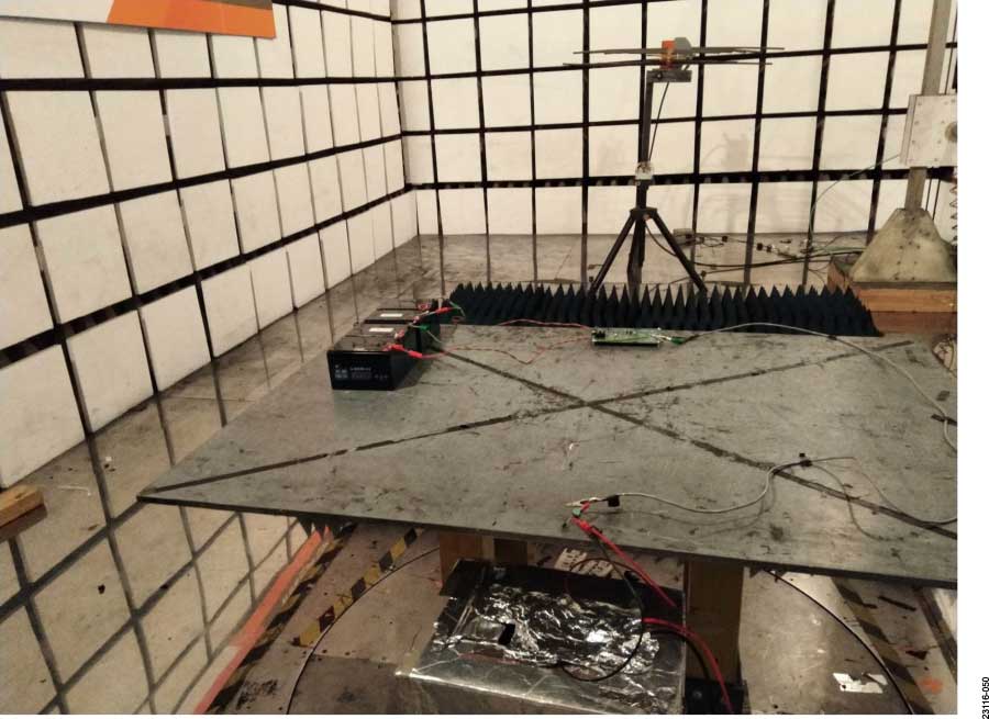


RADIATED EMISSIONS
Per the CISPR 11 standard, the EUT is placed on top of a rotating table, 0.8 m above the ground, in a 10 m, semianechoic chamber. The table is rotated 360° to identify the position of the highest radiation. The EUT is set 10 m from the interference receiving antenna, which can be set to a horizontal or vertical polarization position. The antennas are mounted on top of a variable height antenna tower. The heights of the antennas vary from 1 m to 4 m above the ground to identify the maximum value of the field strength. The EUT is configured to its typical worst case where the antenna is tuned to a height from 1 m to 4 m, and the table is turned from 0° to 360° to find the maximum reading. The typical worst case for the EUT means that the AD5758 is being refreshed at 1 kHz at its full-scale voltage or current output. The test receiver system is set to quasipeak detection mode. The EUT is powered by two 24 V dc battery packs. Any radiated emission from the auxiliary supply can be excluded.
The AN-1599 describes the AD5758 EMC test board, which shares the same blank PCB of this AD5758 and ADP1031 EMC test board but is assembled with partially different BOM that implements the power and digital isolation with discrete ICs. The AD5758 EMC test board has emission peaks around 205 MHz, which does not satisfy the 6 dB margin against CISPR 11 Class B. The AD5758 and ADP1031 EMC test board in contrast is not only 10 dB lower around the frequencies but also has a very low emissions profile in the range of 30 MHz to 230 MHz where the CISPR 11 Class B limit is more stringent, mainly due to the higher integration and design optimizations of the ADP1031 for EMI.
| Frequency (MHz) | Result (dBμV) | Limit (dBμV) | Margin (dB) | Height (cm) | Degree (°) | Antenna Polarity | Remark |
| 31.9400 | 21.68 | 30 | −8.32 | 203 | 361 | Vertical | Peak detection |
| 143.4900 | 17.49 | 30 | −12.51 | 100 | 237 | Vertical | Peak detection |
| 359.8000 | 22.33 | 37 | −14.67 | 100 | 157 | Vertical | Peak detection |
| 597.4500 | 26.28 | 37 | −10.72 | 399 | 357 | Vertical | Peak detection |
| 776.9000 | 28.95 | 37 | −8.05 | 199 | 0 | Vertical | Peak detection |
| 823.4600 | 29.54 | 37 | −7.46 | 300 | 33 | Vertical | Peak detection |
| 30.0000 | 21.85 | 30 | −8.15 | 200 | 320 | Horizontal | Peak detection |
| 330.7000 | 20.11 | 37 | −16.89 | 101 | 213 | Horizontal | Peak detection |
| 551.1200 | 24.43 | 37 | −12.57 | 400 | 327 | Horizontal | Peak detection |
| 680.8700 | 32.86 | 37 | −4.14 | 101 | 287 | Horizontal | Peak detection |
| 680.9500 | 27.16 | 37 | −9.84 | 101 | 275 | Horizontal | Quasi peak |
| 790.4800 | 29.98 | 37 | −7.02 | 101 | 2 | Horizontal | Peak detection |
| 914.6400 | 29.97 | 37 | −7.03 | 300 | 362 | Horizontal | Peak detection |
| Frequency (MHz) | Result (dBμV) | Limit (dBμV) | Margin (dB) | Height (cm) | Degree (°) | Antenna Polarity | Remark |
| 30.0000 | 22.93 | 30 | −7.07 | 100 | 309 | Vertical | Peak detection |
| 348.1600 | 22.97 | 37 | −14.03 | 100 | 135 | Vertical | Peak detection |
| 467.4700 | 23.96 | 37 | −13.04 | 300 | 259 | Vertical | Peak detection |
| 649.8300 | 27.43 | 37 | −9.57 | 200 | 84 | Vertical | Peak detection |
| 777.8700 | 29.40 | 37 | −7.60 | 399 | 262 | Vertical | Peak detection |
| 923.3700 | 29.20 | 37 | −7.80 | 100 | 251 | Vertical | Peak detection |
| 30.9700 | 21.34 | 30 | −8.66 | 300 | 360 | Horizontal | Peak detection |
| 356.8900 | 21.49 | 37 | −15.51 | 300 | 241 | Horizontal | Peak detection |
| 599.3900 | 26.73 | 37 | −10.27 | 300 | 360 | Horizontal | Peak detection |
| 681.5000 | 27.93 | 37 | −9.07 | 101 | 183 | Horizontal | Quasi peak |
| 683.7800 | 32.35 | 37 | −4.65 | 101 | 243 | Horizontal | Peak detection |
| 821.5200 | 28.78 | 37 | −8.22 | 101 | 191 | Horizontal | Peak detection |
| 889.4200 | 28.38 | 37 | −8.62 | 400 | 221 | Horizontal | Peak detection |


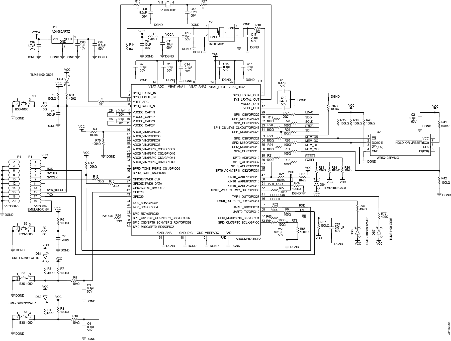
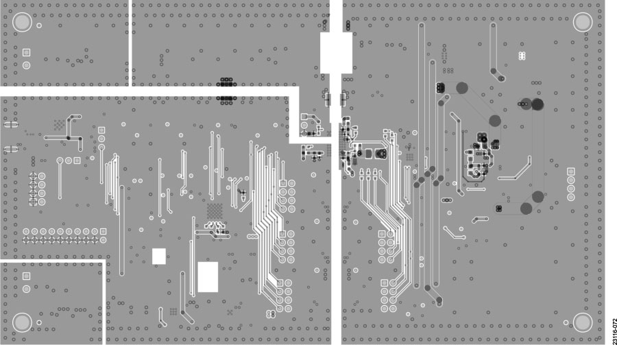
EMC BOARD SCHEMATICS AND ARTWORK


ORDERING INFORMATION
BILL OF MATERIALS
| Reference Designator | Part Description | Part Number | Manufacturer |
| C1, C2, C13, C17 | Capacitor, ceramic, C0G (NP0), general-purpose, 20 pF | GRM1885C1H200JA01D | Murata |
| C3 to C7, C10, C14 to C16, C21, C23, C27 to C29, C32, C33, C35, C46, C52, C55, C64, C68, C80, C81, C117, C119 to C121, C128, C141 | Capacitor, ceramic, X7R, 0603, 0.1 μF | 06035C104KAT2A | AVX |
| C175,C176,C177 | Capacitor, ceramic, X7R, general-purpose, 0.01 μF | GRM155R71E103KA01D | Murata |
| C178 | Capacitor, ceramic, NP0, general-purpose, 22 pF | CC0402JRNPO9BN220 | YAGEO |
| C122 | Multilayer ceramic capacitor (MLCC) for high voltage, X7R, 3300 pF | HV1812Y332KXHATHV | Vishay |
| C9,C11 | Capacitor, ceramic, X5R, general-purpose, 10 μF | GRM31CR61H106KA12L | Murata |
| C22, C24, C25, C30,C31, C45, C82, C118 | MLCC, X5R, 4.7 μF | C2012X5R1H475K125AB | TDK |
| C8, C12 | Capacitor, ceramic, 8.2 pF | 06035A8R2CAT2A | AVX |
| C39, C125 | Capacitor, ceramic, X7R, high voltage, 0.001 μF | C1812C102KHRACTU | Kemet |
| C130 | Capacitor, ceramic, X7R, soft termination, 0.01 μF | C1608X7R1H103K080AE | TDK |
| C53, C131, C133, C138, C142 to C144 | Capacitor, ceramic, X7R, 0.01 μF | GCM155R71H103KA55D | Murata |
| C18, C19 | Capacitor, ceramic, X7R, 0.47 μF | C1608X7R1H474MT | TDK |
| C26 | MLCC, X5R, 10 μF | C2012X5R1V106K085AC | TDK |
| C34 | Capacitor, ceramic, X7R, 2.2 μF | UMK212BB7225KG-T | Taiyo Yuden |
| C37, C44, C47 to C49, C54 | Capacitor, ceramic, X7R, general-purpose, 2.2 μF | GRM31CR71H225KA88L | Murata |
| C38 | Capacitor, ceramic, NP0, 220 pF | CC0603JRNPO9BN221 | Yageo |
| C40, C41, C95, C96 | Capacitor, ceramic, NP0, 0.001 μF | 12065A102JAT2A | AVX |
| C50 | Capacitor, ceramic, C0G (NP0), general-purpose, 0.002 μF | GRM2165C1H202JA01D | Murata |
| C56, C57 | Capacitor, ceramic, X7R, general-purpose, 0.01 μF | GCG188R71H103KA01D | Murata |
| C62 | Capacitor, ceramic, X5R, general-purpose, 4.7 μF | GRM21BR61E475KA12L | Murata |
| C63 | Capacitor, ceramic, X7R, 1 μF | 0603YC105KAT2A | AVX |
| D4, D10 | Diode, general-purpose, rectifier | S2M | ON Semiconductor |
| D5, D6, D11, D12 | Diode, TVS, bidirectional | SMCJ33CA-TR | ST Microelectronics |
| D16 | Diode, TVS, bidirectional | SMAJ33CA-TR | ST Microelectronics |
| D2 | Diode, Schottky Rectifier | BAT46W-7-F | Diodes Incorporated |
| DS1, DS2, DS5, DS6 | LED, SMD, 0603,green | SML-LX0603GW-TR | Lumex |
| DS3, DS4, DS7 | LED, SMD, 0603, red | TLMS1100-GS08 | Vishay |
| E1, E2, E3, E4 | Inductor, ferrite bead, 1 .5kΩ, 100 MHz | BLM18HE152SN1D | Murata |
| E5, R68, R166, R167 | Resistor, thick film, chip, 1210, 0 Ω | CRCW12100000Z0EAHP | Vishay |
| FL1 | Filter, EMI, common-mode, 30 dB, 0.1 A, 8 Ω | EMI2121MTTAG | ON Semiconductor |
| JP25, JP26 | Connector, PCB, header jumper, 1 × M000385 | 22-03-2031 | Molex |
| L1, L6, L8 | Ferrite bead ,SMD, 120 Ω, 120 nH | LI0805H750R-10 | Laird |
| L2, L3 | Inductor, power choke, 100 μH | LPS5030-104MRB | Coilcrft |
| L5 | Inductor, shielded power, 47 μH | LPS4018-473MRB | Coilcraft |
| P1 | Connector, PCB, header, low profile | 5103308-5 | TE Connectivity LTD |
| P2, P14 | Connector, PCB, terminal block, two position, green | 1727010 | Phoenix Contact |
| P3 | Connector, PCB, receptor, mini USB 2.0 | UX60SC-MB-5S8 | Hirose |
| P4 | Connector, PCB, four position terminal block, single-row, straight, 2.54 mm pitch, 3.5 mm tail length | 1725672 | Phoenix Contact |
| P8, R1, R2, R14, R16 to R18, R60, R164, R170, R173 | Resistor, thick film, chip, 0603, 0 Ω | MC0603WG00000T5E-TC | Multicomp |
| R9, R10, R36, R37, R143, R152, R154 R155 | Resistor, thick film, chip, 0603, 10 kΩ | MC0100W0603110K | Multicomp |
| R19 to R21, R23, R24, R27 to R32, R47 to R54, R62 to R65 | Resistor, thick film, chip, 0603, 100 Ω | MC0.063W06031100R | Multicomp |
| R3, R4, R11, R33, R61, R76, R77 | Resistor, thick film, chip, 0603, 499 Ω | ERJ-3EKF4990V | Panasonic |
| R5 to R8, R12, R22, R25, R26, R34, R35, R38, R40 to R42, R66, R67, R74, R75, R141, R151, R163, R168, R171, R182 | Resistor, thick film, chip, 0603, 100 kΩ | ERJ-3EKF1003V | Panasonic |
| R138 | Resistor, thick film, chip, 0603, 1 MΩ | ERJ-3EKF1004V | Panasonic |
| R139 | Resistor, thick film, chip, 0603, 210 kΩ | ERJ-3EKF2103V | Panasonic |
| R89 | Resistor, thick film, chip, 0402, 0 Ω | MC00625W040210R | Multicomp |
| R13, R15, R92 to R94, R140, R142, R148 | Resistor, thick film, chip, 0603, 33 Ω | MC0.063W0603133R | Multicomp |
| R43 | Resistor, thick film chip, 0603, 31.6 kΩ | ERJ-3EKF3162V | Panasonic |
| R44, R46 | Resistor, thick film, chip, 0603, 560 kΩ | MC 0.063W 0603 1% 560K | Multicomp |
| R45 | Resistor, thick film, chip, 0603, 23.2 kΩ | ERJ-3EKF2322V | Panasonic |
| R56, R145 | Resistor, thick film, chip, 0603, 1 kΩ | MC0063W060311K | Multicomp |
| R176, R177 | Resistor, thin film, chip, 0805, 0 Ω | MC0.1W08050R | Multicomp |
| R180, R181 | Resistor, thick film, chip, 0603, 2 kΩ | MC0.063W060312K | Multicomp |
| R55 | Resistor, precision, thin film, 0603, 13.7 kΩ | RN73C1J13K7BTG | TE Connectivity |
| R57 | Resistor, thick film, chip, 0805, 10 Ω | ERJ-6ENF10R0V | Panasonic |
| R58 | Resistor, thick film, high voltage, chip, 4.7 MΩ | CHV2010-JW-475ELF | Bourns |
| S1 to S4 | Switch, surface mount, SMT | B3S1000 | Omron |
| T1, T3 | Common-mode choke, DLW5BS series, 190 Ω, 5 A | DLW5BSN191SQ2L | Murata |
| T2 | Flyback transformer, 1:1 ratio, 280 μH, 250 mA | 750316743 | Würth Elektronik |
| U1 | IC, ultra low power, Arm Cortex-M3, MCU | ADuCM3029BCPZ | Analog Devices |
| U11 | IC, micropower, precision, series mode, voltage reference | AD1582ARTZ | Analog Devices |
| U13 | IC, TTL, single, two input positive and gate | SN74LVC1G08DBVT | Texas Instruments |
| U2 | IC, 3 V, 128 Mb, serial flash memory with dual/quad SPI and quick path interconnect (QPI) | W25Q128FVSIG | Winbond |
| U26 | IC, TTL, single, two-input, positive and gate | SN74AHCT1G08DCKR | Texas Instruments |
| U3 | IC, isolated micro power management unit and digital isolator, adjustable VOUT1, 5.15 V VOUT2, adjustable VOUT3 | ADP1031ACPZ-1-R7 | Analog Devices |
| U4 | IC, single-channel, 16-bit, current/voltage output DAC, dynamic power control, HART connectivity | AD5758BCPZ-REEL | Analog Devices |
| U6 | IC, low noise, CMOS, LDO regulator, 5 V voltage output | ADP7142ARDZ-5.0 | Analog Devices |
| U7 | IC, USB, serial universal asynchronous receiver/transmitter (UART) | FT232RQ | FTDI |
| U8 | IC, low quiescent current, CMOS linear regulator, 3.0 V voltage output | ADP124ARHZ-3.0-R7 | Analog Devices |
| U9 | IC, micropower voltage reference, 2.5 V voltage output | ADR3425ARJZ-R7 | Analog Devices |
| Y1 | IC, crystal, SMD, 12.5 pF, 32.7680 kHz | MC-306-32.7680K- A0:ROHS | Seiko |
| Y2 | IC, crystal, ultraminiature ceramic sealed, 10 pF, 26.000 MHz | ABM8G-26.000MHZ- B4Y-T | Abracon |
Author
