ADL8140
RECOMMENDED FOR NEW DESIGNS10 GHz to 18 GHz Low Noise Amplifier
- Part Models
- 4
- 1ku List Price
- Starting From $47.15
Part Details
- Self biased, single positive supply LNA
- Resistor-adjustable bias current
- Internally matched and AC-coupled
- Frequency range: 10 GHz to 18 GHz
- Noise figure: 1 dB from 12 GHz to 15 GHz
- Gain: 27.5 dB from 12 GHz to 15 GHz
- RoHS-compliant, 2 mm × 2 mm, 8-lead LFCSP
The ADL8140 is a low noise amplifier (LNA) that operates from 10 GHz to 18 GHz.
Typical gain and noise figure are 27.5 dB and 1 dB, respectively, from 12 GHz to 15 GHz. Output power for 1 dB compression (OP1dB) and output third-order intercept (OIP3), are 8 dBm and 23 dBm, respectively, from 12 GHz to 15 GHz. The nominal quiescent current (IDQ), which can be adjusted, is 35 mA from a 1.5 V supply voltage (VDD). The ADL8140 also features inputs/outputs that are AC-coupled and internally matched to 50 Ω.
The ADL8140 is housed in a RoHS-compliant, 2 mm × 2 mm, 8-lead lead frame chip scale package [LFCSP] and is specified for operation from −55°C to +125°C.
Documentation
Data Sheet 2
User Guide 1
Application Note 2
High Dose Rate Radiation Reports 1
ADI has always placed the highest emphasis on delivering products that meet the maximum levels of quality and reliability. We achieve this by incorporating quality and reliability checks in every scope of product and process design, and in the manufacturing process as well. "Zero defects" for shipped products is always our goal. View our quality and reliability program and certifications for more information.
| Part Model | Pin/Package Drawing | Documentation | CAD Symbols, Footprints, and 3D Models |
|---|---|---|---|
| ADL8140ACPZN | 8-lead LFCSP 2 mm × 2 mm × 0.85 | ||
| ADL8140ACPZN-CSL | 8-lead LFCSP 2 mm × 2 mm × 0.85 | ||
| ADL8140ACPZN-R7 | 8-lead LFCSP 2 mm × 2 mm × 0.85 | ||
| ADL8140ACPZN-R7-CSL | 8-lead LFCSP 2 mm × 2 mm × 0.85 |
This is the most up-to-date revision of the Data Sheet.
Software Resources
Can't find the software or driver you need?
Request a Driver/SoftwareTools & Simulations
S-Parameter 1
Evaluation Kits
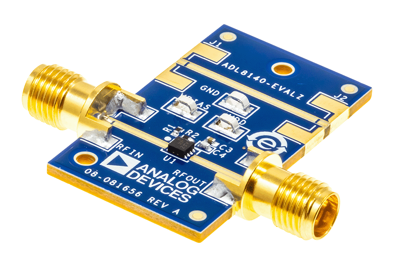


Evaluating the ADL8140 GaAs, pHEMT, MMIC, Low Noise Amplifier, 10 GHz to 18 GHz
Resources
Latest Discussions
No discussions on ADL8140 yet. Have something to say?
Start a Discussion on EngineerZone®