ADN4656

RECOMMENDED FOR NEW DESIGNS

5 kV RMS/3.75 kV RMS, Dual LVDS Gigabit Isolator (First Channel Reversed)

Part Models
4
1ku List Price
Starting From $7.18
Viewing:

Part Details

  • 5 kV rms and 3.75 kV rms LVDS isolators
  • Complies with TIA/EIA-644-A LVDS standard
  • Multiple dual-channel configurations
  • Any data rate up to 1.1 Gbps switching with low jitter
    • 4 ns typical propagation delay
    • 2.6 ps rms typical random jitter, rms
    • 90 ps typical peak-to-peak total jitter at 1.1 Gbps
  • 2.5 V or 3.3 V supplies
  • −75 dBc power supply ripple rejection, phase spur level
  • Glitch immunity
  • ±8 kV IEC 61000-4-2 ESD protection across isolation barrier
  • High common-mode transient immunity: >25 kV/μs
  • Passes EN 55022 Class B radiated emissions limits with 1.1 Gbps PRBS
  • Safety and regulatory approvals (20-lead SOIC_W package)
    • UL (pending): 5000 V rms for 1 minute per UL 1577
    • CSA Component Acceptance Notice 5A (pending)
    • VDE certificate of conformity (pending)
      • DIN V VDE V 0884-10 (VDE V 0884-10):2006-12
      • VIORM = 424 VPEAK
  • Fail-safe output high for open, short, and terminated input conditions (ADN4655/ADN4656)
  • Operating temperature range: −40°C to +125°C
  • 7.8 mm minimum creepage and clearance
ADN4656
5 kV RMS/3.75 kV RMS, Dual LVDS Gigabit Isolator (First Channel Reversed)
ADN4656 Functional Block Diagram ADN4656 Pin Configuration
Add to myAnalog

Add product to the Products section of myAnalog (to receive notifications), to an existing project or to a new project.

Create New Project
Ask a Question

Documentation

Learn More
Add to myAnalog

Add product to the Products section of myAnalog (to receive notifications), to an existing project or to a new project.

Create New Project

Tools & Simulations


Evaluation Kits

eval board
EVAL-ADN4656

ADN4656 Evaluation Board

Features and Benefits

  • Isolated ground planes (logic side and bus side)
  • Convenient connections through SMA terminals
    • 3.3 V or 2.5 V power on Side 1 (VIN1 and VDD1) and Side 2 (VIN2 and VDD2)
    • Ground on Side 1 (GND1) and ground on Side 2 (GND2)
    • LVDS input signals: DIN1+, DIN1−, DIN2+, DIN2−
    • LVDS output signals: DOUT1+, DOUT1−, DOUT2+, DOUT2−
  • Jumper-selectable power supply of 3.3 V or 2.5 V
  • Termination resistors on all LVDS drivers and receivers

Product Details

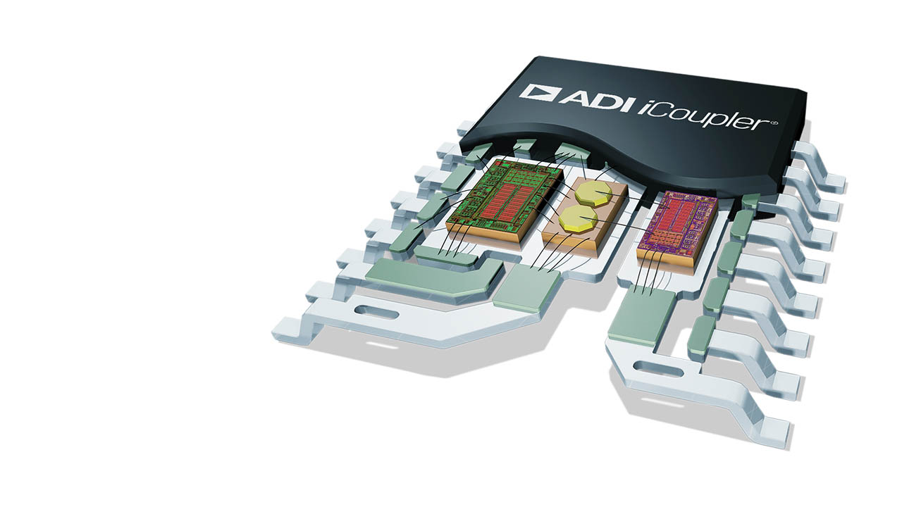
The EVAL-ADN4654EB1Z, the EVAL-ADN4655EB1Z, and the EVAL-ADN4656EB1Z allow quick and easy evaluation of the ADN4654/ADN4655/ADN4656 low voltage, differential signaling (LVDS) isolators without the need for external components. The ADN4654/ADN4655/ADN4656 employ Analog Devices, Inc., iCoupler® technology to combine a 2-channel isolator with an LVDS receiver and driver into a single, 20-lead wide body SOIC package. The devices are capable of running at data rates of up to 1.1 Gbps with low jitter.

The evaluation boards have separate ground and power planes for each side of the isolator. This separation enables the evaluation of the ADN4654/ADN4655/ADN4656 with galvanic isolation between both sides of the device. Jumper-selectable power supplies at 3.3 V or 2.5 V are required on each side of the ADN4654/ADN4655/ADN4656 device. Using an on-chip, low dropout (LDO) regulator, 2.5 V can be provided from an external 3.3 V power supply.

Complete information about the ADN4654/ADN4655/ADN4656 is available in the ADN4654/ADN4655/ADN4656 data sheet. Consult this data sheet in conjunction with this user guide when using the evaluation boards.

EVAL-ADN4656
ADN4656 Evaluation Board
EVAL-ADN4656EB1ZTOP-web EVAL-ADN4656EB1ZBOTTOM-web EVAL-ADN4656EB1ZANGLE-web

Latest Discussions

Recently Viewed