AD3552R
RECOMMENDED FOR NEW DESIGNSDual Channel, 16-Bit, 33 MUPS, Multispan, Multi-IO SPI DAC
- Part Models
- 2
- 1ku List Price
- Starting From $37.45
Part Details
- 16-bit resolution
- 33 MUPS single channel rate in fast mode
- 22 MUPS single channel rate in precision mode
- 65 ns small signal settling time to 0.1% accuracy
- 100ns large signal settling time to 0.1% accuracy
- Ultra small glitch: < 50 pV×s
- Ultra low latency: 5 ns
- THD: −105 dB at 1 kHz
- Highly configurable output voltage span and offset
- 1.2 V and 1.8 V logic level compatible
- Single (classic), dual, and quad SPI modes
- Multiple error detectors, both analog and digital domains
- 2.5 V internal voltage reference, 10 ppm/°C maximum temperature coefficient
- 5 mm × 5 mm LFCSP
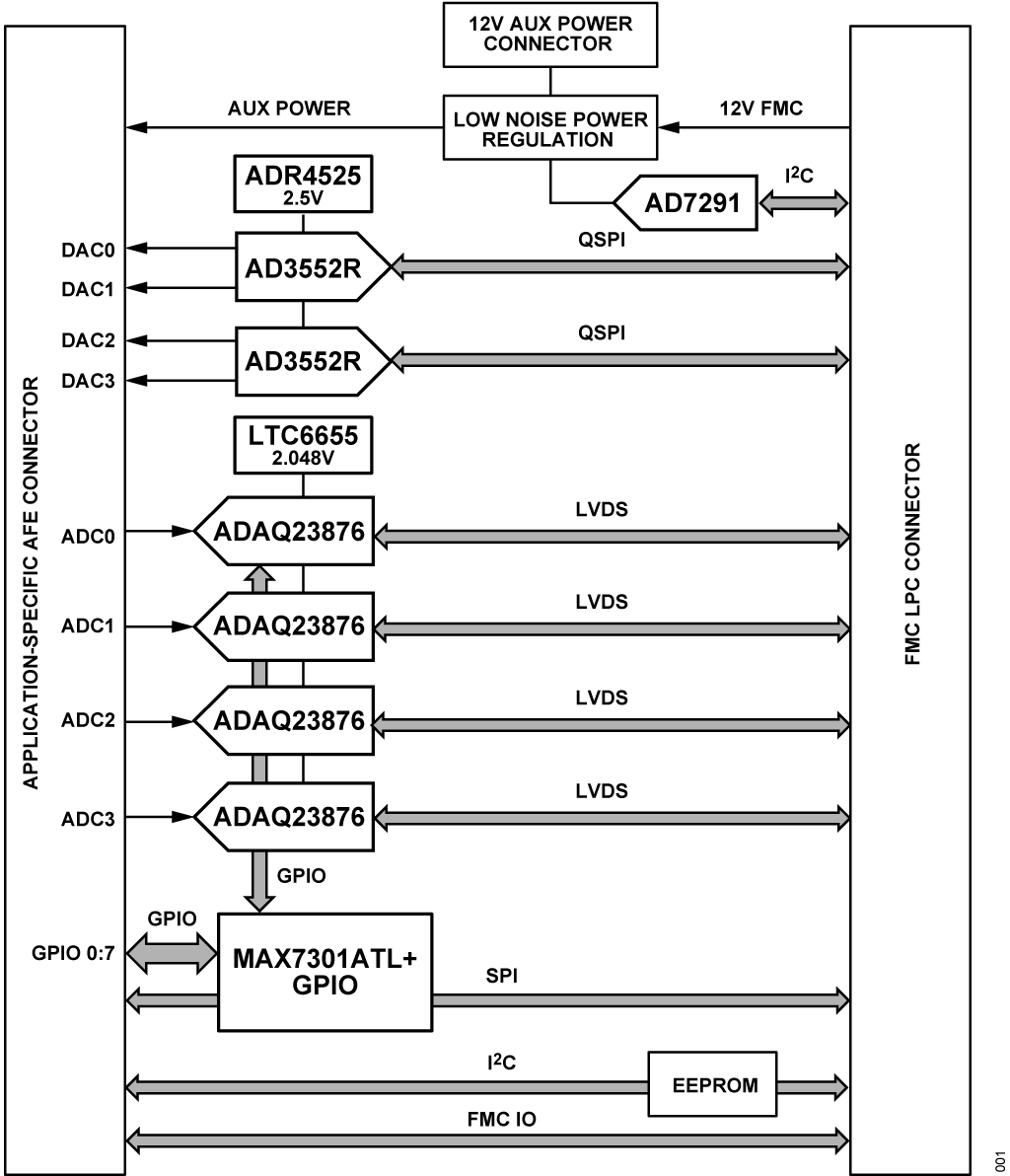
The AD3552R is a low drift, ultra-fast, 16-bit accuracy, current output digital-to-analog converter (DAC) that can be configured in multiple voltage span ranges. The AD3552R operates with a fixed 2.5 V reference.
Each DAC incorporates three drift compensating feedback resistors for the required external transimpedance amplifier (TIA) that scales the output voltage. Offset and gain scaling registers allow for generation of multiple output span ranges, such as 0 V to 2.5 V, 0 V to 5 V, 0 V to 10 V, −5 V to +5 V, and −10 V to +10 V, and custom intermediate ranges with full 16-bit resolution.
The DAC can operate in fast mode for maximum speed or precision mode for maximum accuracy.
The serial peripheral interface (SPI) can be configured in quad SPI mode, dual synchronous SPI mode, dual SPI mode, and single SPI (classic SPI) mode with single date rate (SDR) or double data rate (DDR), with logical levels from 1.2 V to 1.8 V.
The AD3552R is specified over the extended industrial temperature range (–40°C to +105°C).
APPLICATIONS
- Instrumentation
- Hardware in the loop
- Process control equipment
- Medical devices
- Automatic test equipment
- Data acquisition system
- Programmable voltage sources
- Optical communications
Documentation
Data Sheet 1
User Guide 1
Video 2

Device Drivers 6
Webcast 5
ADI has always placed the highest emphasis on delivering products that meet the maximum levels of quality and reliability. We achieve this by incorporating quality and reliability checks in every scope of product and process design, and in the manufacturing process as well. "Zero defects" for shipped products is always our goal. View our quality and reliability program and certifications for more information.
| Part Model | Pin/Package Drawing | Documentation | CAD Symbols, Footprints, and 3D Models |
|---|---|---|---|
| AD3552RBCPZ16 | 32-Lead LFCSP (5mm x 5mm x 0.95mm w/ EP) | ||
| AD3552RBCPZ16-RL7 | 32-Lead LFCSP (5mm x 5mm x 0.95mm w/ EP) |
This is the most up-to-date revision of the Data Sheet.
Software Resources
Mbed Support 1
Device Drivers 6
Evaluation Software 0
Can't find the software or driver you need?
Hardware Ecosystem
Tools & Simulations
LTspice 1
Models for the following parts are available in LTspice:
- AD3552R
IBIS Model 1
LTspice® is a powerful, fast and free simulation software, schematic capture and waveform viewer with enhancements and models for improving the simulation of analog circuits.
Evaluation Kits


RF Front-end GaN Power Amplifier Biasing, Protection, and Control Reference Design
Resources
Software


Evaluation Board for the AD3552R-16 which is a low drift ultrafast, 16-bit accuracy, current output digital-to-analog converter (DAC)