CN0534


Overview
Design Resources
Design & Integration File
- Schematic
- Bill of Materials
- Gerber Files
- Assembly Drawings
- Allegro Layout File
Evaluation Hardware
Part Numbers with "Z" indicate RoHS Compliance. Boards checked are needed to evaluate this circuit.
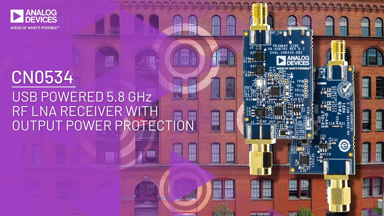
- EVAL-CN0534-EBZ ($48.15) 5.8 GHz ISM Band Low Noise Receive Amplifier
Device Drivers
Software such as C code and/or FPGA code, used to communicate with component's digital interface.
Features & Benefits
- 23.5 dB Gain
- 5.8 GHz Optimized LNA
- ISM Band Operation
- USB Powered
Markets and Technologies
Parts Used
Documentation & Resources
Circuit Function & Benefits
The International Telecommunication Union (ITU) allocates the un-licensed 5.8 GHz industrial, scientific, and medical (ISM) radio frequency band for use worldwide. Advancements in wireless technologies and standards, as well as minimal regulatory compliance requirements, have made this frequency band popular for short range, wireless communication systems.
The 5.8 GHz band is preferred for short range digital communication applications (such as WiFi) because of the number of channels and the bandwidth available. While the transmission range is short-er than that of the 2.4 GHz band, its 150 MHz bandwidth accommodates up to 23 non-overlapping WiFi channels. Additional com-mon uses include software defined radio, wireless access points, public safety radio, wireless repeaters, femtocells, and Long-Term Evolution (LTE)/Worldwide Interoperability for Microwave Access (WiMAX)/4G, base transceiver station (BTS) infrastructure.
This design provides high gain, robust overpower monitoring, and protection all in a small footprint, which is a great addition to any ISM band application where low signal strength or distance may be a complication.
The circuit shown in Figure 1 is a high performance RF receiver system with +23 dB of gain, optimized for operation at a center frequency of 5.8 GHz. The input is unfiltered, maintaining a noise figure of 2 dB, while a bandpass filter at the output attenuates out-of-band interferers.
The circuit includes a high speed overpower detector and switch that protects sensitive downstream equipment connected to the receiver system. The receiver system also automatically returns to normal operation when the RF power level drops within the acceptable range. The RF inputs and outputs are standard SMA connectors, and the entire design is powered from a single micro USB connector.

Circuit Description
RF Low Noise Amplifier (LNA)
The HMC717A is a gallium arsenide (GaAs), pseudomorphic high electron mobility transistor (PHEMT), monolithic microwave IC (MMIC), LNA that is ideal for back-end receivers operating between 4.8 GHz and 6.0 GHz for various signal communication protocols such as ISM, MC-GSM, W-CDMA, and TD-SCDMA.
As shown in Figure 2, the HMC717A has a gain of 14.5 dB through its RF band of operation. The noise figure is 1.1 dB and the amplifier is powered from a single 5 V supply with a total supply current of 68 mA. In order to achieve an overall gain of 23 dB, two HMC717A amplifiers are cascaded. The 1.1 dB noise figure, 27 dBm third-order intercept point (IP3), and 15 dB compression point (P1dB) make the HMC717A suitable for both the first stage LNA and intermediate gain stage.


LNA Impedance Matching
As show in Figure 3, the RFIN (Pin 2) and RFOUT (Pin 11) pins of the HMC717A are single-ended with a nominal impedance of 50Ω over the 4.8 GHz to 6.0 GHz frequency range, allowing the HMC717A to be directly interfaced with a 50Ω terminated system without requiring additional impedance matching circuitry.
The RFOUT has an integrated DC blocking capacitor that elimi-nates the need for an external capacitor at the second stage, enabling multiple HMC717A amplifiers which be cascaded back to back without the need for external matching circuitry. The only requirement is that RFIN of the first stage must be AC-coupled with a 1.2 pF capacitor.

Band-Pass Filter
The LNA output is filtered by a band-pass filter. As shown in Figure 4, the filter has a pass band from 5400 MHz to 6400 MHz with a return loss of 14.7 dB typical and an insertion loss of 1.6 dB at a 5.8 GHz center frequency.


Overpower Protection
Sensitive circuitry can be damaged by relatively low power levels. For example, the RF inputs of the AD9363 transceiver have an absolute maximum power level of +2.5 dBm. The CN0534 includes an overpower protection with automatic reset circuitry for when the power level drops within the acceptable range, as shown in Figure 5.

RF Power Detector and Auto Retry Circuitry
The ADL5904 is an RF power detector that operates from DC to 6 GHz. The input of the ADL5904 is recommended to have a 470 nF ac coupling capacitor along with an external 82.5Ω shunt resistor to provide a wide band input match. The ADL5904 uses an internal RF envelope detector and user defined input voltage to provide a programmable threshold detection function based on the RF input power level. When the voltage from the RF envelope detector exceeds the user defined threshold voltage at the VIN− pin, the internal comparator latches the event to a flip flop. The response time from the RF input signal exceeding the user programmed threshold, to the output latching is a very fast 12 ns. The latched event is held on the flip flop until a reset pulse is applied to the RST pin.
The power level at the output of the band-pass filter on the CN0534 is sampled by an integrated thin film coupler with a coupling factor of +13 dB and forwarded to the RFIN pin of the ADL5904. The ADL5904 threshold level on VIN− is set by a resistor divider with a value set at approximately 32 mV, which is equivalent to a −9 dBm threshold power when operating uncalibrated at 5.8 GHz as indicated in the ADL5904 data sheet. Combined with the losses of the coupler and RF attenuator in the 0 dB state, the output is kept at a safe level for sensitive devices.
If higher overpower threshold precision is required, a simple calibration routine can be performed at multiple frequencies to compensate for device-to-device variations within the system. Refer to the ADL5904 data sheet for information on the calibration routine.
The Q output of the ADL5904 holds an LTC6991programmable low-frequency timer in reset during normal operation. When an overpower event occurs, the LTC1991 is enabled and a 4 ms delay begins. The ADL5904 is reset after 4 ms, effectively re-sampling the power level. If the overpower condition persists, the ADL5904 trips again and the attenuator is held in the -20 dB state. The attenuator control signal is delayed, such that it remains in the -20 dB state continuously as the power level is re-sampled. If the overpower condition has subsided, the attenuator returns to the 0 dB state and normal operation resumes, as show in Figure 6.

RF Attenuator
The HMC802A is a broadband bidirectional 1-bit GaAs IC digital attenuator. This device features low insertion loss of 1.5 dB at 5.8 GHz in bypass mode and an accurate 20±0.6 dB attenuation when enabled. Operating from a single 5 V supply, the IP3 is +55 dBm and the attenuation control signal is CMOS/TTL compatible. While an RF switch would typically be used in an overpower protection application, at 5.8 GHz the HMC802A's 20 dB attenuation is better than the off-state isolation of most RF switches.
Shown in Figure 7, the device performance with typical insertion loss in bypass mode is 1.5 dB at 5.8 GHz center frequency. Figure 8 shows an isolation of -20.5 dB in attenuation mode at 5.8 GHz center frequency.


Combining the insertion loss from the band pass filter, coupler and from the RF attenuator, this results in a total insertion loss of approximately 3 dB at the output of the RF attenuator in normal operating conditions and approximately 21.5 dB when operating in attenuation mode at a center frequency of 5.8 GHz.
Protection Results
The overpower protection functionality was tested using the setup shown in Figure 9. An RF signal generator was set to 5.8 GHz output frequency and the power to the input of the CN0534 was ramped from -30 dBm to -20 dBm. The CN0534 output power was monitored with an ADL6010 high-speed envelope detector, which provides an accurate measurement of the response time from the overpower event to the output power being attenuated.


Once tripped, the detector latch is reset at a frequency of 250 Hz, and the output switch is enabled if the output power has dropped to less than 2.5 dBm. The switch enable signal is delayed ensuring that it is not asserted if the overpower condition is still present. Both results can be seen in Figure 10 and Figure 11.
USB Power Management
Boost Converter
Figure 12 shows the EVAL-CN0534-EBZ power tree, which consumes 1.1 W of power from the 5 V supply available on the micro USB jack.

The LT8335 is a current mode DC/DC converter capable of generating either positive or negative output voltages using a single feedback pin. It can be configured as a boost, SEPIC or inverting converter consuming as low as 6µA of quiescent current. Low ripple Burst Mode operation maintains high efficiency down to very low output currents while keeping the output ripple below 15 mV in a typical application. The internally compensated current mode architecture results in stable operation over a wide range of input and output voltages. Integrated soft-start and frequency foldback functions are included to control inductor current during start-up. Shown in Figure 13 are the basic connections needed to configure the LT8335 for a 5.6 V output.
The output voltage is programmed with a resistor divider from the output to the FBX pin. Choose the resistor values for a positive output voltage according to Equation 1:

Ultralow Noise Linear Regulator

The 5 V output from the ADM7150, an ultralow noise, high PSSR, RF linear regulator, is used to maximize the gain of the HMC717A. The ADM7150 is a low dropout linear regulation with a typical output noise of 1.0 µV rms from 100 Hz to 100 kHz for fixed output voltage options and <1.7 nV/√Hz noise spectral density above 10 kHz, as is shown in Figure 14.


The ADP150 is used to generate 3.3 V for the power detector and auto retry circuit. As shown in Figure 15, it is a high performance low dropout linear regulator featuring an ultralow noise and ultra high PSRR architecture for powering noise sensitive RF applications.


Common Variations
For wider bandwidth of operation, the HMC8411 can be used as an alternative part for the RF LNA. The HMC8411 is low noise wideband amplifier that operates from 0.01 GHz to 10 GHz. It provides a typical gain of 15.5 dB, a 1.7 dB typical noise figure, and a typical output third-order intercept (OIP3) of 34 dBm, requiring only 55 mA from a 5 V supply voltage. The HMC8411 also features inputs and outputs that are internally matched to 50 Ω, making the device ideal for surface-mounted technology (SMT)-based, high capacity microwave radio applications.
An HMC550A can be an alternate part for the RF switch. It is a low-cost single pole single throw (SPST) failsafe switch used in applications which require low insertion loss and low current consumption. These devices can control signals from DC to 6 GHz and are especially suited for IF and RF applications including RFID, ISM, automotive and battery powered tags and portables.
For an envelope detector, an ADL6010 can be an alternative part which is a fast responding, 45 dB range, 0.5 GHz to 43.5 GHz envelope detector. The ADL6010 is a versatile, broadband envelope detector covering the microwave spectrum. It features very low power consumption (8 mW) in a simple, easy to use 6-lead format. The output is a baseband voltage proportional to the instantaneous amplitude of the radio frequency (RF) input signal. It exhibits minimal slope variation of the RF input to envelope output transfer function from 0.5 GHz to 43.5 GHz.
Circuit Evaluation & Test
The following section describes the general test setup for evaluating the CN0534 performance. For complete details, see the CN0534 User Guide.
Equipment Needed
- The EVAL-CN0534-EBZ reference design board
- An RF signal source (R&S® SMA100B)
- A signal source analyzer (Keysight E5052B SSA)
- A network analyzer (Keysight N5242A PNA-X)
- A SMA to SMA cable
- A micro USB to USB cable
- A 5 V ac/dc USB power adapter
Test Setup

To measure the phase noise and SFDR shown in Figure 16, take the following steps:
- Set the measurement configuration of the signal source as follows:
- For SFDR measurement, set the center frequency = 5.8 GHz, the frequency span = 5.79 GHz to 5.81 GHz, and the RF amplitude = 10 dBm.
- For phase noise measurement, set the center frequency = 5.8 GHz and the offset frequency range = 10 Hz to 30 MHz. Refer to the maximum input level on the signal source analyzer data sheet if the equipment can handle the amplifier output (~20 dBm at a 0 dBm input). If necessary, connect an attenuator to the input of the signal source analyzer.
- Set the power level of the signal source generator to 0 dBm with a center frequency set at 5.8 GHz.
- Power up the EVAL-CN0534-EBZ using the micro USB cable with the 5V power adapter rated for greater than 500 mW.
- Connect the signal generator output to the RF input (J2) of the EVAL-CN0534-EBZ.
- Connect the RF output (J1) of the EVAL-CN0534-EBZ to the signal source analyzer.
- Execute a measurement run on the signal source analyzer.

To measure the S-parameters and the noise figure shown in Figure 17, take the following steps:
- Set the desired measurement conditions of the vector network analyzer with the following settings:
- For S-parameter measurement, set the frequency span = 4.8 GHz to 6.8 GHz.
- For the phase noise measurement, set the frequency span = 5.3 GHz to 6.8 GHz.
- Perform a full 2-port calibration of the vector network analyzer using a calibration kit. Note that the RF input (J2) of the EVAL-CN0534-EBZ can be connected directly to a test port so that only one measurement cable is needed for the test setup.
- Power up the EVAL-CN0534-EBZ using the 5 V power adapter and microUSB cable.
- Connect the EVAL-CN0534-EBZ across the test ports of the vector network analyzer using the calibrated test setup.
- Set the measurement to the desired S-parameter.
- Execute the autoscale function on the vector network analyzer. Adjust the scale after, if desired.
RF Performance
The EVAL-CN0534-EBZ amplifies the RF signal input by approximately +23 dB gain with a return loss of −15 dB at a 5.8 GHz center frequency. Figure 18 and Figure 19 show the gain and return loss of the EVAL-CN0534-EBZ respectively.


The single sideband phase noise at 5.8 GHz is shown in Figure 20.


Figure 21 shows the narrow-band single tone RF output with a SFDR of roughly 78 dBFS.


Figure 22 shows the corresponding noise figure versus frequency that shows approximately 2 dB at the 5.8 GHz center frequency.

