Introduction: An Engineer’s Challenges in Evolving Times
Sometimes power design is left as an afterthought for PCB applications, with compressed time schedules forcing engineers to overlook crucial details, other than the standard VIN, VOUT, and load requirements. Unfortunately, the missed details can appear in PCB production as hard-to-diagnose problems. For instance, after a lengthy debugging process, the designer finds the circuitry randomly misbehaves, say, due to switching noise. The source of random errors can be very difficult to pinpoint.
This article is the first of a 2-part series that addresses some of the issues sometimes overlooked when designing multirail power supplies. Part 1 focuses on the strategy and topology, while Part 2 focuses on the specifics of power budgeting and board layout, along with some tips and tricks. As many application boards use power to bias a number of logic levels, this article series examines a multisupply board solution. The goal is to achieve a correct first-time design topology or strategy.
So Many Choices
For any particular power supply design, there are many possible solutions. In the examples that follow, several options are described, such as single-chip supply vs. multivoltage rail integrated circuits (ICs). Cost and performance trade-offs are assessed. The trade-offs of low dropout (LDO) regulators vs. switching regulators (often known as buck or boost regulators) are covered. Hybrid methods (that is, a mix and match of LDO regulators and buck regulators), including voltage input to output control (VIOC) regulator solutions, are also included.
In this article, we look at switching noise and how, if a switched power supply design is not adequately filtered, the PCB circuitry can be impacted. Other design considerations include cost, performance, implementation, and efficiency from a top-level design perspective.
For example, how can one best design with respect to multisupply topologies based on a given source or sources? From this, we’ll dive into the designs, the IC interface technology, the voltage threshold levels, and what type of regulator noise impacts the circuitry. We will cover some fundamental logic levels, such as 5 V, 3.3 V, 2.5 V, and 1.8 V transistor-to-transistor logic (TTL), complementary metal oxide semiconductors (CMOS), and their respective threshold requirements.
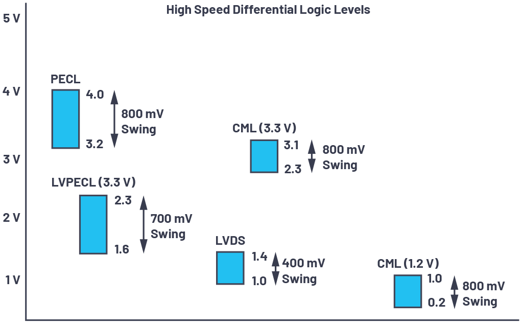
Advanced logic, such as positive emitter couple logic (PECL), low voltage PECL (LVPECL), and current-mode logic (CML), is mentioned but not covered in detail. These examples are very high speed interfaces, and low noise levels are important for these. Designers need to be aware of how to avoid these issues due to signal swings.
In power supply design, cost and performance often come hand-in-hand, so the designer must carefully consider the logic levels and the requirements for clean power. By designing for robustness and the headroom available in regard to tolerance and noise, production problems can also be avoided.
A designer needs to be aware of the trade-offs with respect to power supply design: what is achievable vs. what is acceptable. If a design doesn’t achieve the required performance, then the designer must examine options and the cost to bring it to spec. For instance, a multirail device, such as the ADP5054, may meet required performance advantages while remaining cost-effective.
A Typical Design Example
Let’s start with a design example. Figure 1 shows a block diagram for a board that takes the incoming 12 V and a 3.3 V as the main supply source. The main supplies must be stepped down to produce 5 V, 2.5 V, 1.8 V, and possibly the 3.3 V for applications on the PCB. If the external 3.3 V can provide sufficient power and sufficiently low noise, then the 3.3 V incoming rail can be used without further regulation to avoid extra cost. If not, the 12 V incoming rail could be used to provide sufficient power by stepping it down to the required 3.3 V for PCB apps.


An Overview of the Logic Interface
Multiple power supplies are typical for PCBs. An IC may operate using 5 V alone; or it may require multiple supplies that use 5 V and 3.3 V for the input/output interface, 2.5 V for the internal logic, and 1.8 V for low power sleep mode. Low power mode might be always on, used for logic such as timer functions, housekeeping logic, or for wake-up mode upon interrupts or the IRQ pin to enable and power the IC—that is, the 5 V, 3.3 V, and the 2.5 V supplies. Some or all of these logic interfaces are often used inside an IC.
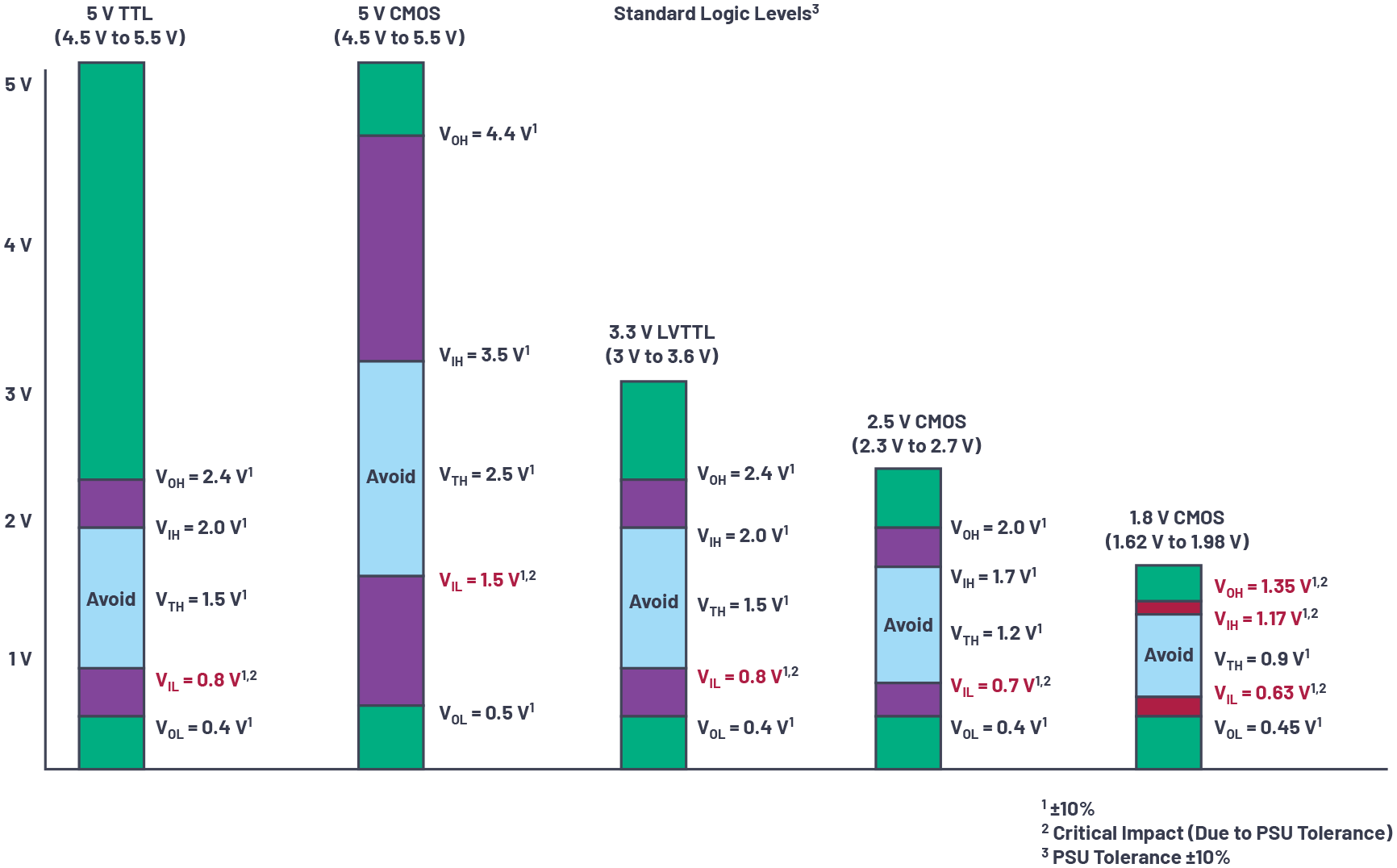
The standard logic interface levels in Figure 2 show various TTL and CMOS threshold logic levels and their acceptable input and output voltage logic definitions. In this article, we are interested when the input logic is driven low, as denoted by voltage input low (VIL), and when driven high, as denoted by input logic level high (VIH). In particular, we focus on VIH, the threshold uncertainty area marked “Avoid” in Figure 2.
In all cases, a ±10% power supply tolerance must be factored in. Likewise, Figure 3 shows high speed differential signals. For the purpose of this article, we will focus on the standard logic levels shown in Figure 2.

Switching Noise
When not well-filtered, switching regulator buck or boost power supply designs can produce switching noise in tens of millivolts to hundreds of millivolts, with possible spikes of 400 mV to 600 mV. It is important to know if switching noise is a problem for the logic levels in play and for the interface.
Safety Margin
To ensure a proper safety margin for a robust PSU, a design rule of thumb is to work with the worst-case scenario of –10% tolerance. For example, a 5 V TTL VIL of 0.8 V becomes 0.72 V and 1.8 V CMOS VIL of 0.63 V becomes 0.57 V, and the threshold voltage (VTH) lowers accordingly (5 V TTL VTH = 1.35 V and 1.8 V CMOS VTH = 0.81 V). Switching noise (VNS) can be tens of mV to hundreds of mV. Furthermore, the logic circuitry itself features signal noise (VN)—that is, interference noise. The total contribution noise voltage, VTN = VN + VNS , can be in the range of 100 mV to 800 mV. When VTN is added to the nominal signal to create the total signal voltage (VTSIG ): the actual total signal, VTSIG = VSIG + VTN , impacts the threshold voltage (VTH), further expanding the avoid region. Signal levels operating within VTH region are indeterminate, where logic circuitry can randomly flip either way; for example, the worst-case scenario results in a falsely triggered Logic 1 instead of a Logic 0.

Multirail PSU Caveats and Tips
By understanding the threshold levels, both at the interface input and the internal logic within the IC, we now know what level can trigger a true logic level or (unintentionally) a false logic level. The question is: how quiet must the supply be to meet these thresholds? Low dropout linear regulators are very quiet, but not necessarily efficient at high step-down ratios. Switching regulators can step down voltages efficiently, but do produce some noise. An efficient and quiet power supply system should probably contain some combination of these two types of power supplies. This article highlights various combinations, including hybrid methods, where an LDO regulator is used after a switching regulator.
An Approach that Maximizes Efficiency and Minimizes Noise (Where Needed)1, 2
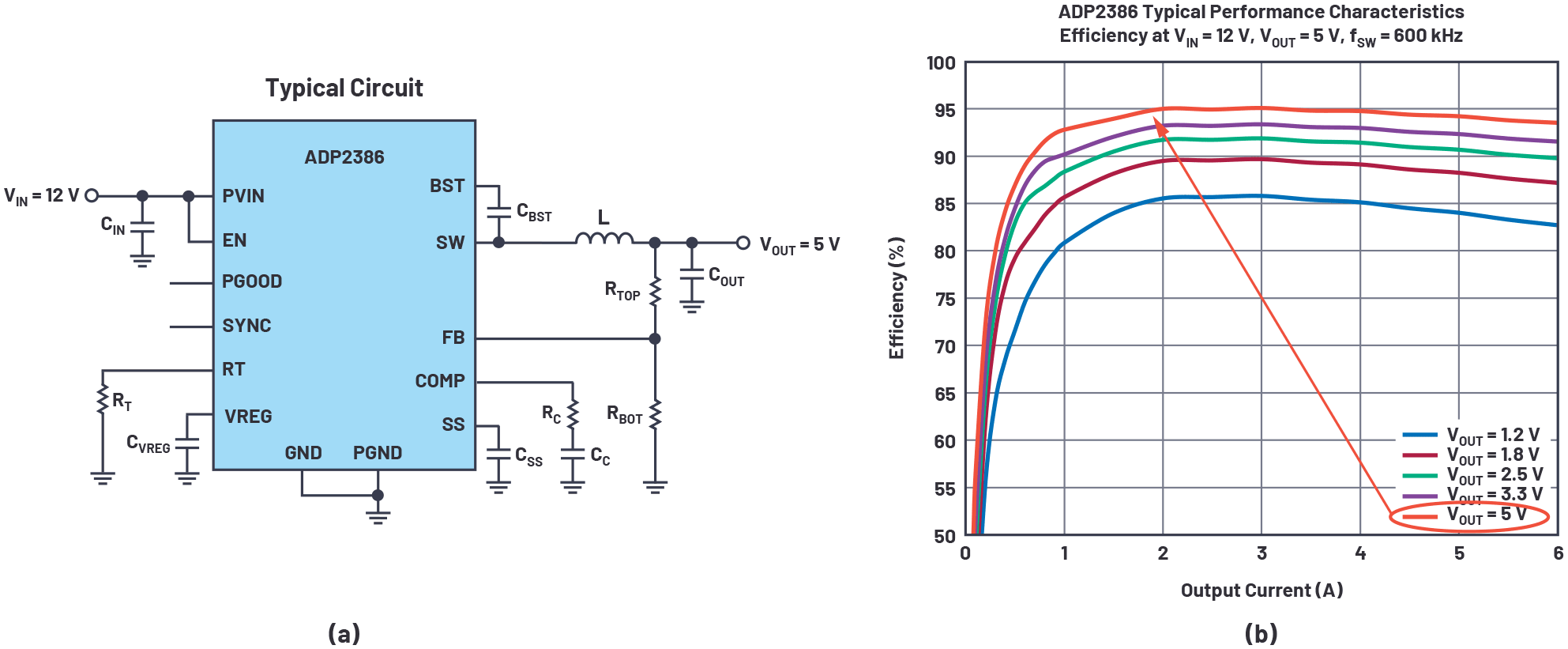
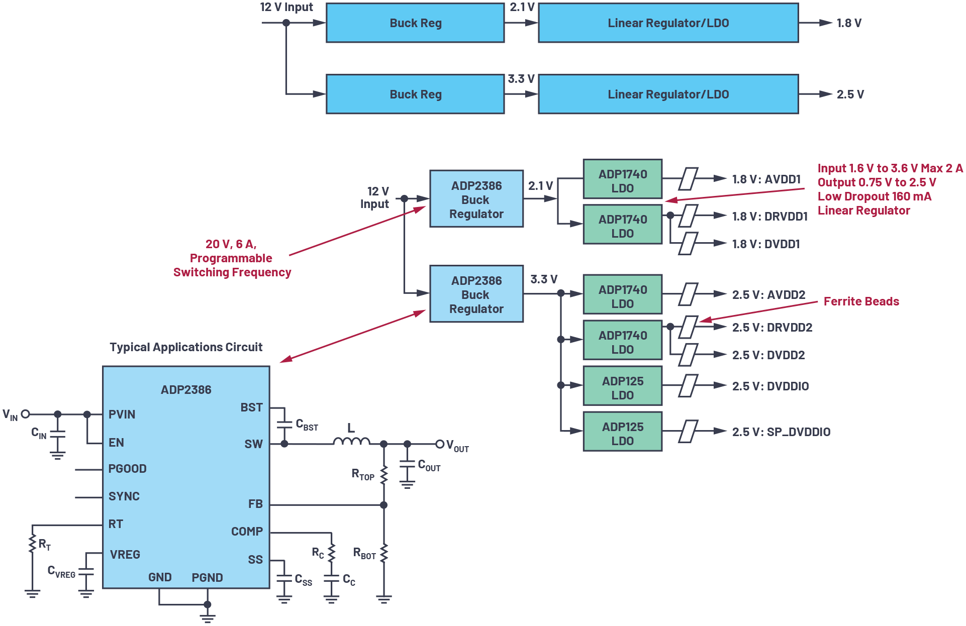
From the design example in Figure 1, to maximize the efficiency and minimize the switching noise for 5 V regulation, tap off the 12 V line and use buck regulators, such as the ADP2386. From standard logic interface levels—the 5 V TTL VIL and the 5 V CMOS VIL are 0.8 V and 1.5 V, respectively—we have allowable margin with just the switching regulators. For these rails, efficiency is maximized by using a buck topology, while switching noise remains below the VIL in the 5 V (TTL and CMOS) technology. Using a buck regulator, such as the ADP2386 configuration shown in Figure 4a, the efficiency can be as high as 95% as shown in ADP2386’s typical circuit and efficiency plot (see Figure 4b). If a relatively quiet LDO regulator was used for this design, the 7 V drop from VIN to VOUT would result in significant internal power dissipation in the form of heat and lost efficiency. For a robust design, with a small additional cost, having an LDO regulator after a buck regulator to produce the 5 V is an added benefit.


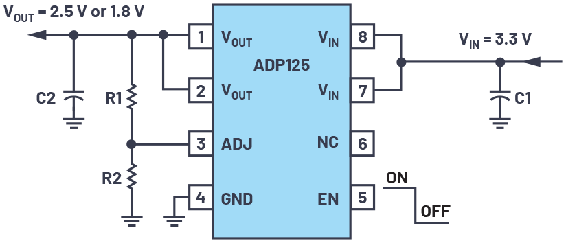
The VIL for 2.5 V and 1.8 V CMOS are 0.7 V and 0.63 V, respectively. Unfortunately, the safety margin for this logic level is not enough to avoid switching noise. To solve this problem, two options are available. The first option is that, if the incoming external 3.3 V supply as shown in Figure 1 has sufficient power and is very low noise, then tap off this external 3.3 V and use a linear regulator (LDO regulator) such as the ADP125 (Figure 5) or the ADP1740 for the 2.5 V and 1.8 V supply. Note that there is a 1.5 V drop from 3.3 V to 1.8 V. If this drop is a concern, then a hybrid method can be used. The second option is that, if the external 3.3 V is not low noise or does not have sufficient power, then tap off the 12 V supply by means of a buck followed by an LDO regulator to produce the 3.3 V, the 2.5 V, and the 1.8 V supplies; a hybrid method is shown in Figure 6.
Dropping in an LDO regulator slightly increases cost and board area and adds a little heat dissipation, but these trade-offs are necessary in order to achieve the safety margin. There is a small reduction in efficiency by using LDO regulators, but this can be minimized by keeping a small voltage drop from VIN to VOUT: 0.8 V from 3.3 V to 2.5 V, or 1.5 V from 3.3 V to 1.8 V. Efficiency and transient performance can be maximized using regulators featuring VIOC, which regulates the output of the upstream switching regulator to maintain an optimal voltage drop across the LDO regulator. Examples with the VIOC features include the LT3045, LT3042, and LT3070-1.
The LT3070-1 is a 5 A, low noise, programmable output, 85 mV low dropout linear regulator. If an LDO regulator must be used, then heat dissipation is a concern, where power dissipation = VDROP × I. For example, the LT3070-1 supporting 3 A, a typical value for power drop across the regulator (or power dissipation) is 3 A × 85 mV = 255 mW. Compared to some typical LDO regulators with a dropout of 400 mV, at the same output current of 3 A, the power consumption is 1.2 W—almost five times higher than the LT3070-1.
Alternatively, by using a hybrid method, we can trade cost for efficiency. Efficiency and performance are optimized in Figure 6, where we employ a buck regulator (ADP2386) first to increase the efficiency as much as possible, by regulating it down to the lowest allowable voltage, followed by an LDO regulator (ADP1740).

1This exercise gives a general design example to show some topology and techniques. However, one must not forget to factor in other considerations such as IMAX, cost, package, voltage drops, etc.
2There are also low noise buck and boost regulator options available, such as Silent Switcher® regulators, which have very low noise and low EMI. For example, the LT8650S and LTC3310S can be cost-effective in terms of performance, package, footprint, and layout area.
Package, Power, Cost, Efficiency, and Performance Trade-Offs
Production PCB designs often demand compact multirail supplies for high power, high efficiency, top performance, and low noise. For example, the ADP5054 quad buck regulator offers a high power (17 A), single-chip, multirail power solution for applications such as FPGAs, as shown in Figure 7. The real estate required for the full power supply solution is approximately 41 mm × 20 mm. The footprint for the ADP5054 itself is only 7 mm × 7 mm to deliver 17 A of total current. For very high levels of power in a tight space, consider ADI’s µModule® regulators, such as the LTM4700, which can deliver up to 100 A from a package size of 15 mm × 22 mm.


In Part 2
In Part 2 of this series, we will look at how a cascade strategy is applied at the board level, including selecting proper ICs to account for the power budget and board layout, along with tips and tricks.
References
AD8045 Exposed Paddle Connection. Analog Devices, Inc., January 2011.
Header Pin. Digi-Key Electronics.
Knoth, Steve. “Supply Clean Power with Ultralow Noise LDO Regulators.” Analog Devices, Inc., September 2018.
Kueck, Christian. “Application Note 139: Power Supply Layout and EMI.” Linear Technology, October 2012.
“MT-093 Tutorial: Thermal Design Basics.” Analog Devices, Inc., 2009.
Radosevich, Andy. “Dual Linear Regulator for Digital IC Power Enables On-the-Fly Output Adjustment and Dynamic Headroom Optimization.” Analog Devices, Inc., April 2020.
Zhang, Henry J. “Application Note 136: PCB Layout Considerations for Nonisolated Switching Power Supplies.” Linear Technology, June 2012.
