A New-Generation High Current, High Performance Step-Down and Step-Up Buck-Boost μModule Regulator
A New-Generation High Current, High Performance Step-Down and Step-Up Buck-Boost μModule Regulator
2025-01-01
摘要
This article introduces a new high performance step-up and step-down buck-boost μModule® regulator. It achieves the highest power efficiency and the coolest thermal performance compared to the old generation high current buck-boost μModule regulators. Several other great features, including parallelable configuration for higher power applications, optional constant current regulation, and redundant input configuration, are also introduced.
Introduction
There are many applications with wide input and/or output voltage ranges, such as a battery-powered system. The power supply needs to regulate its output voltage while the input voltage can be lower or higher than the output voltage. A four-switch buck-boost topology can offer the highest efficiency and power density for such an application, as long as ground isolation is not required. Furthermore, a buck-boost power regulator is very flexible and can be used as a buck-only (step-down) or boost only (step-up with short-circuit protection) power supply.
Analog Devices’ µModule group has developed several buck-boost regulators. Figure 1 illustrates the LTM8045, LTM8049, LTM8083, and LTM4693 targeting for lower current applications. High current applications (up to 12 A) are supported by the LTM4607 family, LTM8055 family, and the newly released LTM4712 buck-boost module. The LTM4607/LTM4605/LTM4609 family incorporates the controller and MOSFETs internally, requiring an external power inductor and sensing resistor (RSENSE) on the PCB to form a complete power solution, as depicted in Figure 2.


Alternatively, the LTM8054, LTM8055, and LTM8056 integrate the power inductor and RSENSE into the µModule package, simplifying the design and layout efforts for customers, as highlighted in Figure 3. The LTM8055 family offers a smaller solution size compared to the LTM4607 family, but its output current is constrained by a small-size integrated inductor, therefore limiting thermal and efficient performances.


In 2023, a new high current, four-switch buck-boost regulator, LTM4712, was released. It is a 36 VIN(max), 12 A power module in a high density 16 mm × 16 mm × 8.34 mm BGA package. It integrates a high performance power inductor into the package using advanced ADI proprietary component-on-package technology. Figure 4 shows a proprietary current sensing scheme integrated in the module. This not only saves space but also minimizes additional power loss. Leveraging a cutting-edge buck-boost controller and the advanced ADI package, this device achieves the highest power level, power density, efficiency, and excellent thermal performance across a wide input and output voltage range.


The LTM4712’s fast, cycle-by-cycle current-mode control enables reliable protection and smooth mode transitions. It facilitates excellent current sharing when parallel configurations are employed for higher current applications. Additionally, this new device supports an optional constant output current mode for battery charging applications and allows redundant inputs, enhancing its versatility as a redundant power supply.
Table 1 offers a comprehensive module comparison among the LTM4712, LTM4607 family, and LTM8055 family. The LTM4712 stands out for its high current, power efficiency, and user friendly design, making it an ideal choice for applications where its 8.34 mm height is acceptable.
| LTM4712 | LTM4605 | LTM4607 | LTM4609 | LTM8054 | LTM8055 | LTM8056 | |
| Inductor, RSENSE | Integrated L/DCR |
External L and RSENSE | Integrated L and RSENSE | ||||
| Control Strategy |
Peak current | Valley current for buck Peak current for boost |
Valley current for buck Peak current for boost |
||||
| VIN Range | 5 V to 36 V | 4.5 V to 20 V | 4.5 V to 36 V | 4.5 V to 36 V | 5 V to 36 V | 5 V to 36 V | 5 V to 60 V |
| VOUT Range | 1 V to 36 V | 0.8 V to 16 V | 0.8 V to 24 V | 0.8 V to 34 V | 1.2 V to 36 V | 1.2 V to 3 V | 1.2 V to 48 V |
| IOUT_MAX (Buck) | 12 A | 12 A | 10 A | 10 A | 5.4 A | 8.5 A | 5.5 A |
| IOUT_MAX (6 VIN to 12 VOUT) |
6 A | 5 A | 5 A | 4 A | 1.8 A | 3 A | 1.7 A |
| Package Size (mm) |
16 × 16 × 8.34 (BGA) |
15 × 15 × 2.82 (LGA) | 15 × 15 × 2.82 (LGA) 15 × 15 × 3.42 (BGA) |
15 × 11.25 × 3.4 (BGA) |
15 × 15 × 4.92 (BGA) | ||
| Pin Compatibility |
N/A | Pin-compatible | N/A | Pin-compatible | |||
| Efficiency | Highest | Middle | Lowest | ||||
Significant Efficiency Gain and Thermal Improvements by the LTM4712
Figure 5 illustrates the efficiency comparison among the LTM4607, LTM8055, and the recently introduced LTM4712 under 6 VIN, 12 VIN, and 24 VIN for 12 VOUT conditions. The assessment is conducted using standard evaluation boards available online. Based on the test results, the LTM4712 not only exhibits significantly higher efficiency compared to the other two but also enhances current capability.


In Figure 6, a thermal performance comparison is presented under room temperature conditions without any forced cooling. Remarkably, the LTM4712 maintains a temperature of 30°C lower while doubling the power, in contrast to the LTM8055 under 12 VIN and 12 VOUT. For applications requiring a 12 A current, employing two or three LTM8055 devices in parallel is necessary, depending on the cooling system. On the other hand, a single LTM4712 suffices, significantly reducing PCB footprint and simplifying circuit design.


Table 2 provides a comprehensive overview of efficiency and thermal performance under various operating conditions for the LTM4712, LTM4607, and LTM8055 with an ambient temperature of 25°C and no forced cooling. Figure 7 illustrates the current density in relation to the solution footprint. All tests and comparisons are conducted based on standard demo boards available online.
| Operating Condition |
Parameters | LTM4712 | LTM4607 | LTM8055 |
| 6 VIN/12 VOUT (Boost) |
Max IOUT (A) | 6 | 5 | 3 |
| Efficiency (%)_IMAX |
93.7 | 93.2 | 91.5 | |
| Thermal (°C)_IMAX |
62 | 76 | 80 | |
| 12 VIN/12 VOUT (Buck-Boost) |
Max IOUT (A) | 12 | 10 | 6 |
| Efficiency (%)_IMAX |
96.4 | 95.9 | 93 | |
| Thermal (°C)_IMAX |
80 | 79 | 125 | |
| 24 VIN/12 VOUT (Buck) |
Max IOUT (A) | 12 | 10 | 6 |
| Efficiency (%)_IMAX |
97 | 95 | 93.6 | |
| Thermal (°C)_IMAX |
72 | 93 | 110 |


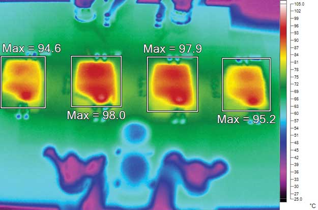
Good Current Sharing in Parallel Configuration
The LTM4712 can be configured in parallel to achieve higher output power with a straightforward setup. Thanks to its current-mode control, it delivers excellent current sharing performance. The EVAL-LTM4712-A2Zevaluation kit showcases the operation of four modules in parallel, providing a total output current of 48 A.
When implementing a parallel configuration with the device, it is essential to refer to the design and configuration of the evaluation board. For effective current sharing, connect the COMP pins and FB pins when paralleling modules. The PHMODE pin can be utilized to configure the phase shift. In a scenario with four modules in parallel, tying the PHMODE pin to INTVCC results in a 90° phase shift, offering optimal interleaving. Additionally, for frequency synchronization, connect the CLOCKOUT signal of the first module to the SYNC pin of the second module.
Figure 8 presents thermal results without forced cooling, revealing consistently similar temperatures across each LTM4712, indicating good current sharing. In Figure 9, the IMON voltage on each device in a 48 A load condition is displayed. The average value for each IMON pin is about 0.7 V, indicating a 12 A load from each channel. These tests are conducted on the evaluation board.


Optional Constant Current Regulation
The LTM4712 can be used as a constant output current source, making it suitable for applications such as battery chargers or LED drivers. In Figure 10, the example circuit depicted is designed to deliver a consistent 10 A load current.


To set the load current, the ISET pin and an external output current sensing resistor near the output are employed. The equation VSENSE = IOUT × RSENSE_IOUT defines the voltage that represents the average output current. The maximum VSENSE is determined by the voltage on the ISET pin ranging from 0.2 V to 1.2 V, corresponding linearly to 0 mV to 50 mV. The ISET pin voltage VISET is established by a 15 μA internal current source and a resistor RISET connected between the ISET pin and ground, represented by VISET = 15 μA × RISET. The output current is then calculated as IOUT = (VISET – 0.2 V)/(20 × RSENSE_IOUT). According to this equation, the output current along with different VISET based on 5 mΩ RSENSE_IOUT is shown as the blue curve in Figure 11. The purple curve shown in Figure 11 is the bench-tested result. As seen, the measured results have a good match with the ideal curve, which demonstrates good accuracy of constant current regulation.


It’s essential to note that the maximum VSENSE is internally limited to 50 mV when the ISET pin is floating or when the ISET pin voltage exceeds 1.2 V. Due to the ripple current in the output, an RC filter must be applied to the ISP and ISN pins for precise average current sensing. Moreover, when selecting the feedback resistor between the FB pin and ground, ensure it results in a higher output voltage than the targeted VOUT.
Redundant Power Supply
The LTM4712 accommodates applications necessitating redundant inputs. It can be utilized for systems requiring backup power supplies or those drawing from distinct input sources to support a common load. Figure 12 illustrates an example circuit where two modules, powered by different inputs (VIN1 and VIN2), collectively deliver a 12 V output with a 24 A load. Notably, any drop-off in either input has no impact on output regulation, and peak inductor current sharing remains effective through the connection of COMP pins.


In Figure 13, bench-tested waveforms under two different conditions are presented. Figure 13a showcases a scenario where both Phase 1 and Phase 2 operate in buck-boost mode. Initially, Phase 1 handles a 4 A load current, gradually sharing half of the load current with Phase 2 upon activation. The IMON waveform confirms equal load current sharing between both phases when both are operational.


Figure 13b replicates the same load condition but with different inputs. Here, Phase 1 operates in boost mode while Phase 2 operates in buck mode. Due to the tied COMP pins, both phases exhibit the same peak inductor current. Consequently, the output current of Phase 1 (boost) is lower than that of Phase 2 (buck). Specific load currents from each phase can be calculated based on parameters such as inductance, switching frequency, VIN, VOUT, and total load current. In this example, Phase 1 provides a 1.4 A load current, while Phase 2 provides 2.6 A.
Design and Simulation Tools
To further simplify users’ design efforts, the LTM4712 is supported in the LTpowerCAD® tool for power component, efficiency, loop compensation, and load transient designs and optimizations, and in the LTspice® software for time-domain dynamic simulations.
Conclusion
The LTM4712 stands out as a fully integrated buck-boost µModule regulator renowned for its exceptional efficiency, high power density, and good thermal performance. Facilitating easy parallelization for higher power applications, it also shows good current sharing capabilities in parallel configurations. It can be adeptly configured to deliver a constant current output, making it feasible for battery charging systems or LED applications. Additionally, its compatibility with redundant input setups further enhances its adaptability.
For comprehensive guidance on implementing the device, it is recommended to refer to the data sheet and the associated evaluation kit design. These resources provide valuable insights and specifications essential for optimizing performance in diverse applications.
关于作者
Wesley Ballar is a senior product applications engineer supporting µModule® products in the Multimarket Applications Group. He has supported the µModule team in various roles since joining Analog Devices in 2016. Wesley re...
Anjan Panigrahy graduated with a degree in electrical and computer engineering from University of Texas at Austin in 2023 with a focus on power electronics. He joined the Multimarket Applications Group supporting µModule® ...
关联至此文章
技术解决方案
{{modalTitle}}
{{modalDescription}}
{{dropdownTitle}}
- {{defaultSelectedText}} {{#each projectNames}}
- {{name}} {{/each}} {{#if newProjectText}}
-
 {{newProjectText}}
{{/if}}
{{newProjectText}}
{{/if}}
{{newProjectTitle}}
{{projectNameErrorText}}
最新视频 21


