Choosing a Precision Amplifier Topology
摘要
The first block in a precision signal chain after the sensor is often an amplifier circuit, which must amplify the signal of interest while maintaining signal fidelity. This article will discuss how to select the appropriate precision amplifier circuit topology for a sensor application, with a specific focus on the operational amplifier, difference amplifier, current-sense amplifier, instrumentation amplifier, and fully differential amplifier.
Introduction
Precision sensors have long been key to measuring much of the physical world. As the variety and quantity of precision-measurement applications increases, engineers are called upon to design systems that can sense ever-smaller amplitude signals in the presence of interferers, while maintaining signal fidelity. This entails not only the selection of the appropriate sensor, but also careful design of the complete signal path—from the sensor through to the data converter—to digitize the analog measurements. So which amplifier topology is best for a given sensor application? The choice requires consideration of the final system objectives and the design priorities for the amplifier circuit.
The first consideration in choosing an amplifier topology is generally to determine if the sensor output (and therefore amplifier input) signal is singleended or differential. Some topology configurations accept a single-ended input signal, and some accept a differential signal. The selection of the best amplifier topology will also depend on if we want the amplifier to output a single-ended or differential signal.
Single-Ended Operational Amplifier Topology
The operational amplifier (op amp) is an extremely versatile amplifier that can be configured for many different operations, hence the name. In the case of an amplifier circuit with a single-ended input and output, a simple op amp circuit with appropriate feedback from a resistor pair would be used. When using a single-ended op amp circuit to amplify a high precision signal, the choice of which topology to use is usually between a non-inverting amplifier and an inverting amplifier (Figure 1). Both circuits utilize a single feedback resistor and single gain resistor.


A simple single-ended input, single-ended output application is shown in Figure 2. Analog Devices’ TMP35 temperature sensor outputs a voltage that is proportional to temperature at a sensitivity of 10 mV/°C. That signal is then connected to a single-ended, non-inverting amplifier circuit, which has a transfer function of VOUT = G × VIN, where G is the closed-loop gain of the circuit and is equal to 1 + (R2/R1). To sense a temperature range of, for example, 0°C to 50°C, the sensor’s full-scale output range would be 10 mV/°C × 50°C = 500 mV. If the sensor output were to drive, for example, an analog-to-digital converter (ADC) with a 5 V full-scale input range, the signal would need to be amplified by a gain of 10 V/V in order to utilize the ADC’s full input dynamic range. This is achieved with the noninverting operational amplifier circuit, where G = 1 + (9 kΩ/1 kΩ) = 10 V/V.


Common-Mode Rejection
When choosing between amplifier topologies, a crucial factor to assess is the amplifier circuit’s capability to effectively reject common-mode input voltage— preventing the signal voltages that are common to both inputs from manifestation at the output—while amplifying the differential input voltage. The common-mode rejection ratio (CMRR) serves as a quantitative measure of an amplifier circuit’s proficiency in this regard. The higher the CMRR, the less error at the output. CMRR is normally represented as the ratio between two gains: the gain of the differential voltage (ADIFF) relative to the gain of the common-mode voltage (ACM) with units in dB.

Recalling that an ideal op amp has a virtual short between the inputs, the signal voltage applied at one input (+IN) will also be present at the other input (–IN); this is the op amp’s common-mode voltage. Modern op amps can have CMRR specifications of 120 dB to 140 dB or even higher. This level of CMRR keeps common-mode error to a minimum, resulting in high precision at the output. For example, if an op amp has a CMRR specification of 140 dB, then only 0.00001% (or 0.1 ppm) of the common-mode voltage at the op amp inputs will show up on the output (VOUT). For a low voltage op amp with a maximum input range of 5 V, the maximum common-mode error at that output would only be 0.5 µV. But using an op amp with a high input-voltage range—for example 50 V—would result in an error of 5 µV on the output. Whether this is an issue or not depends on the system design requirements. If the common-mode error exceeds the acceptable limit for a specific system design, it would be necessary to use a circuit that minimizes that error contribution.
In a non-inverting topology (Figure 1a), the op amp inputs +IN and –IN will be equal to the signal input (VIN) so any increase in signal voltage results in an increase in common-mode voltage at the op amp input pins and an increase in commonmode error at the output will be seen. Alternatively, consider using an inverting amplifier circuit (Figure 1b). In this topology, the +IN input (and therefore the –IN input) is tied to ground. Since the input common-mode voltage is 0 V, any common-mode voltage at the input and resultant common-mode error at the output is avoided.
The Difference Amplifier
Many sensors present their output as a differential signal, where the physical property being measured is represented by the difference between two voltages. One benefit of using a sensor with a differential output is that any voltage from the sensor that occurs on both outputs of the sensor—that is, the common-mode voltage—can be rejected by an amplifier with a differential input and a high common-mode rejection specification.
Besides rejection of the common-mode voltage from the sensor output, there are other benefits to differential signaling in a system. One benefit is that the high common-mode rejection makes the system robust against electromagnetic interference (EMI). External EMI introduces noise to both conductors of the differential signal; this common-mode noise is rejected by the difference amplifier preserving and amplifying the differential signal of interest for an excellent signalto-noise ratio (SNR). Another benefit of differential signaling is that its amplitude is twice as large as a single-ended signal, which equates to a 6 dB increase in SNR. This doubling of the output signal amplitude makes differential-input amplifiers very valuable in applications with a low supply voltage, where there is insufficient voltage range to permit a large signal swing.
The most fundamental topology for amplifying a precision differential signal is the difference amplifier (Figure 3). A difference amplifier accepts a differential input signal, rejects common-mode voltage (VCM), amplifies the differential input voltage (VDIFF), and outputs an amplified, single-ended signal that is proportional to the difference between the two input voltages. Its transfer function is simply VOUT = G × (VDIFF), where VDIFF is (V2 – V1 ) and G is the gain of the amplifier circuit equal to the ratio (R2/R1).


Unlike the single-ended amplifier, the common-mode voltage is the voltage that is common to both inputs into the circuit, V1 and V2, as opposed to the op amp inputs, +IN and –IN. The common-mode voltage is defined as the average of the two input voltages, VCM = (V2 – V1 )/2. For example, with 5 V on V1 and 3 V on V2, the common-mode input voltage would be 4 V and the differential voltage would be 2 V. It is that 2 V differential signal that will be amplified at the output.
As previously mentioned, the common-mode rejection ratio of an amplifier with a differential input is denoted as CMRR = 20 × log10 (ADIFF/ACM). Note that, as the differential gain (ADIFF) increases and the common-mode gain (ACM) decreases, the common-mode rejection improves proportionately with differential gain. This is a significant advantage, allowing us to achieve both higher gain and improved CMRR simultaneously. One other point to note is that CMRR decreases as frequency increases, so it is important to select a difference amp with the required rejection at the signal frequency of interest.
Resistor Tolerance and Amplifier Precision
The CMRR of a difference amplifier circuit is extremely dependent on how well the ratios of R2/R1 and R2’/R1’ are matched. This can be difficult to achieve when the amplifier circuit is comprised of discrete components, like the one shown in Figure 3. For example, a precision op amp can have a CMRR specification of 140 dB or more. But even if it is an ideal op amp, utilizing it in a 4-resistor difference amplifier circuit, which uses resistors with 0.1% tolerance and has a gain of 1, the circuit can achieve a minimum CMRR of only 54 dB.1 A CMRR of 54 dB is approximately equivalent to the precision of only a 9-bit ADC. Although this may suffice for some applications, high precision applications require much better CMRR and therefore better resistor matching. Another important specification of the amplifier circuit is gain accuracy. To amplify a signal for a specific gain, specific resistor values would be chosen for R2, R1, R1’, and R2’. Any tolerance away from the nominal resistor values results in ratio mismatch and therefore gain error. Since all resistors change resistance with temperature, there is a commensurate error from gain drift over temperature. These issues with a discrete amplifier circuit can be mitigated by very well-matched resistor networks like, for example, the Analog Devices’ LT5400 family with resistor ratio matching of 0.01% or the LT5401 with 0.003% matching.
For the highest level of precision, all these challenges—reduced CMRR, increased gain error, and increased gain drift—as well as other issues like temperature gradients on the printed circuit board, parasitic capacitance, etc., are greatly mitigated by use of an integrated difference amplifier, where the amplifier and resistors are fabricated on a monolithic integrated circuit (IC). Because the resistor values on each IC are precisely matched during production, integrated difference amplifiers have very high CMRR specifications and very low gain error. Also, since they reside on the same die and are made from the same material, each resistor will tend to be close to the same temperature and have the same temperature coefficients so they will exhibit a similar change in resistance over temperature, which results in very little change in resistor ratios and therefore minimal gain drift. Many integrated difference amplifiers have a CMRR specification as high as 80 dB to 90 dB or more, a gain error of 0.005% to 0.02%, and gain drift as low as 1 ppm/°C.
Consider ADI’s integrated LT1997-1 difference amplifier, shown in Figure 4. It has an exceptional specified minimum CMRR of over 100 dB, or about 17 bits of precision. Its typical gain error is ±0.01% and typical gain drift vs. temperature is an ultralow ±0.2 ppm/°C. As an extra benefit, the integration of multiple integrated resistors of different values gives a system designer the option of configuring for different gains. In the case of the LT1997-1, the multiple integrated resistors allow configuration for 24 unique amplification (and attenuation) gains from 0.141 V/V to 80 V/V using no external components.


Current Sensing with a Difference Amplifier
A very popular application of difference amplifiers is precision current sensing, an example of which is shown in Figure 5. The current to the load passes through a very low resistance shunt (sense) resistor. The voltage across the shunt resistor is directly proportional to the load current. The current being sensed generates a small, proportional differential voltage across the shunt resistor. That small voltage is amplified in order to utilize the full input voltage range of an analog-to-digital converter.


The circuit in Figure 5 is referred to as high-side current sensing because the shunt resistor is placed (current is being measured) between the power supply and the load rather than low side sensing where the shunt resistor would be located between the load and ground. There are many advantages to high-side current sensing, one of which is that it can detect a short circuit to ground at the load.
In the case of high-side differential current sensing, two voltages must be considered: the differential voltage (VDIFF), which is the signal voltage between input V2 and input V1 (the voltage across the shunt resistor), and the common-mode voltage (VCM), which is present on both V2 and V1 . In this example, the op amp’s +IN input sees a voltage VSUPPLY (or VLOAD + VDIFF) and the op amp’s –IN input sees VLOAD (or VSUPPLY – VDIFF). The difference amplifier will amplify the difference voltage and reject the common-mode voltage.
In many applications, including high-side current sensing, the common-mode input voltage can be much greater than the amplitude of the differential voltage. In fact, it can often be much greater than the supply voltages of the op amp— sometimes as high as hundreds of volts. As the common-mode error at the output is directly proportional to the common-mode voltage at the input, it follows that systems with exceptionally high common-mode input voltage necessitate a correspondingly high CMRR to attain a precise analog output signal. One of the key attributes of a difference amplifier is that it can reject high commonmode voltages, well beyond the supply voltage range. This is possible because the resistor network on each input attenuates the input voltages V1 and V2 to the point that op amp inputs +IN and –IN are within the specified input voltage range. For example, ADI’s AD8479 accepts common-mode input voltages of ±600 V with supply voltages of ±15 V.
Level Shifting
An additional benefit of a difference amplifier circuit is that it is very easy to level shift the output voltage. Many difference amplifiers include a reference input for this purpose. Applying a voltage to a reference input pin will set the output to that voltage when the difference between the inputs is zero. This capability allows us to align the amplifier output with a chosen reference voltage, such as half of the supply voltage for bidirectional sensing with a single supply (Figure 6) or the midpoint of an ADC’s input voltage range for optimal dynamic range (Figure 7).


For instance, if there is a signal oscillating between ±2.5 V and the goal is to feed this signal into an ADC with a 0 V to 5 V input voltage range, it is desirable to center the signal at half of the ADC’s full-scale input voltage range to make use of the entire input range. Figure 7 illustrates the straightforward method to achieve this. Alternatively, a single voltage can be applied to both REF input pins to directly establish the output reference voltage.
The Current-Sense Amplifier
As discussed earlier, the monolithic difference amplifier is ideal for many applications, one of the most common being current sensing using a low resistance shunt resistor. While there are many current-sensing applications for which difference amplifiers are ideal, there are other applications that benefit from the optimization of certain features and specifications offered by a current-sense amplifier (CSA). These specialty amplifiers typically have a different architecture than difference amplifiers. Instead of an input resistor network that attenuates the input voltage, a CSA often uses high voltage input transistors to directly accept large and rapidly changing common-mode voltages while precisely amplifying small differential current shunt voltages (Figure 8).


In a difference amplifier, the input differential signal is internally attenuated by the resistor network and is then amplified to its original input level plus even more gain to achieve final signal amplification at the output. Restoring the attenuated input to the original signal amplitude consumes some of the internal amplifier’s gain-bandwidth product, giving up some bandwidth for that extra gain. Since the high voltage input transistors of most CSAs don’t attenuate the signal, no gain is required to restore the signal amplitude and the internal op amp has more bandwidth available with which to amplify signal. For example, the small signal –3 dB bandwidth of the AD8206 difference amplifier is 100 kHz, whereas the bandwidth of the AD8210 current-sense amplifier is 450 kHz. The increased bandwidth of a CSA makes it very well suited for higher frequency applications or when detecting fast current transients.
CSAs also tend to have higher common-mode rejection, in the range of 100 dB to 120 dB or more, compared to most difference amplifiers with a CMRR of 80 dB to 100 dB. Note that one trade-off for the greater bandwidth of CSAs is that they don’t have an internal attenuation network and therefore cannot accept the very high levels of common-mode input voltage that a difference amplifier can—although CSA common-mode voltage limits are still very high, in the range of 80 V to 100 V.
CSAs are often used to measure large switching currents. When measuring switching currents (that is, the differential voltage across the shunt resistor) on the high-side of a load, the common-mode voltage at the shunt resistor can often change rapidly between ground and the supply voltage. The rapid change in common-mode voltage can induce large transients at the input to the amplifier. These common-mode voltage transients can often exceed the signal amplitude. Ideally, the amplifier would produce an output that reflects only the amplified differential sense voltage. Practically, a common-mode step response can occur at the output. CSAs specialize in rejecting the common-mode transient spikes from such fast-changing common-mode voltage steps, making them ideal for current sensing of signals with rapid changes in amplitude.
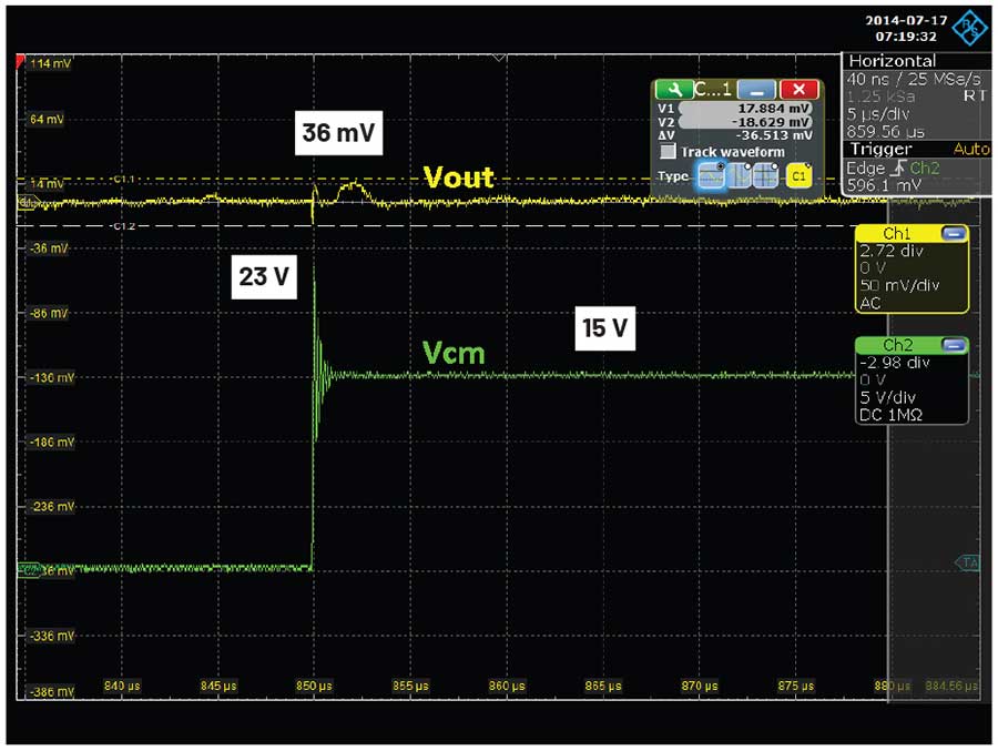
Figure 9 shows the step response and transient rejection achieved by ADI’s AD8418 CSA. The common-mode input voltage is 15 V and the amplifier sees an input transient that overshoots the common-mode voltage by more than 50%. The resulting common-mode step response appears as a brief output perturbation of only 36 mV.

One example where fast switching of the common-mode voltage occurs is in measurement of the phase current in a typical 3-phase motor control system where a controller drives a pulse-width modulation (PWM) signal to the inverter stage, which then drives each leg of the motor (Figure 10). Shunt resistors are placed in line with the motor. Differential voltage feedback of the instantaneous current measurement across the shunt resistors allows the controller to determine the phase of each signal. With each PWM pulse, the common-mode voltage at the shunt resistor is stepping rapidly through the full supply range, between V– and V+. These fast PWM steps require an amplifier that has high bandwidth and can reject the high transient overshoot at the rising and falling edge. ADI’s AD8411A incorporates a precision internal resistor divider network at the input with a common-mode voltage range up to 70 V, features a high 2.7 MHz bandwidth, and includes de-glitch circuitry to enable output accuracy by mitigating the effects of the fast-switching input signal, making it very well suited for this application.


The Instrumentation Amplifier
The differential-input amplifier topologies that have been discussed so far—the difference amplifier and the current-sense amplifier—are excellent at amplifying differential signals in a wide variety of applications, especially where there is a very high common-mode voltage present. For applications requiring the amplification of extremely small signals with exceptional precision amid substantial common-mode voltages, including noise, the use of amplifiers with even greater precision becomes essential. Instrumentation amplifiers (in-amps) are specifically designed for these demanding applications.
Comparing a difference amp to an in-amp, one potential limitation of a difference amp is that they have relatively low input impedance. Another limitation is that the impedance into each amplifier input is not equal. To see where these limitations matter, consider the amplification of a differential signal (V2 – V1 ) from a Wheatstone bridge (Figure 11), which is a configuration that is used in a wide variety of sensors. A first concern is that many bridges have significant output impedance that will be driving a relatively low amplifier input impedance. Using values such as a bridge output impedance of 4 kΩ and a difference-amplifier input impedance of 200 kΩ would mean that 2% of the transducer signal would be lost across its output impedance, which would eliminate any precision measurement. A second concern is that the difference amplifier’s unequal input impedances will cause a difference in voltage drop across each of the two legs of the bridge circuit, resulting in an error in the differential voltage. To solve these issues, it is necessary to use an amplifier that has a much higher input impedance, presents a balanced load on the bridge outputs, and has excellent CMRR. These are the key features and advantages of an instrumentation amplifier.


Looking at the classic 3-op amp instrumentation amplifier (Figure 12a), the two op amps A1 and A2 comprise the first stage (called the pre-amp stage) and a third op amp A3 is used in the second stage (called the subtractor). The subtractor stage is recognizable as the familiar difference amplifier topology. Amplifiers A1 and A2 provide a balanced and extremely high input impedance. They also amplify the differential input voltage and pass the common-mode voltage through without amplification. The subtractor stage at A3 rejects the common-mode voltage and passes the amplified differential voltage to the output. Another feature of this topology is that the system designer can set the gain with a single external resistor (RG), eliminating the need to match discrete resistor ratios. This topology is excellent at amplifying very small signals and rejecting high common-mode voltage. The transfer function of this instrumentation amplifier is VOUT = G × (VDIFF) + VREF, where VDIFF is (V+IN – V+IN), G is the gain of the in-amp, and VREF is the voltage applied to the REF input that level shifts the output voltage.


As with difference amplifiers, integrated in-amps (Figure 12b) benefit from having precisely matched resistors on a monolithic die. Whereas common-mode rejection of an integrated difference amplifier might be in the range of 90 dB to 100 dB, many in-amps have a CMRR specification of 130 dB to 140 dB or more. In the previous bridge example, considering a bridge source resistance of 4 kΩ and, for instance, ADI’s AD8422 in-amp with a 200 GΩ input resistance, the source signal loss is a very small 0.000002% (0.02 ppm). Finally, in-amps tend to have much lower input bias current than difference amps. As a result, there will be less voltage error generated as the input bias currents flow through any source resistance.
The Fully Differential Amplifier
Amplifier topologies with both single and differential inputs have been explored, all featuring single-ended outputs. In a precision signal amplifier circuit design, there may be a necessity to produce a differential output signal. Amplifiers with both differential inputs and outputs are termed fully differential amplifiers (sometimes abbreviated as FDA or diff-amp). Integrated FDAs are versatile, capable of amplifying either single-ended or differential input signals. FDAs excel in rejecting input common-mode voltage, amplifying differential input voltage, and delivering a differential output signal. The output common-mode voltage (VOCM) is determined by applying the desired voltage level to a reference input pin.
A very common application for FDAs is to drive the differential input of a high performance ADC. In this case, they can be used to amplify a small input signal or attenuate a large input signal to within the ADC’s input voltage range. Figure 13 shows ADI’s AD8475 FDA receiving a differential input signal from the sensor and then driving the differential input of a 24-bit, 250 kSPS sigma-delta ADC, the AD7176-2. In this application, the amplifier’s VOCM input is being driven by the ADC’s reference output to set the common-mode voltage at the optimal level for the ADC’s input dynamic range.


Another very popular use for FDAs is to convert a single-ended input signal to a differential output signal. Many sensors output a high precision, single-ended signal. When amplifying or attenuating the signal and subsequently driving a differential ADC input, it is desirable to convert the single-ended signal to a differential one. FDAs are well-suited for this task. Figure 14 illustrates this configuration, grounding one amplifier input and driving the other input with a single-ended signal. Besides conditioning the signal for the ADC’s differential input, converting to a differential output provides the benefit of doubling the signal amplitude (6 dB), resulting in a higher SNR and improved effective resolution of the digitized signal.


Conclusion
The best choice of amplifier topology for a precision signal-conditioning circuit depends on several considerations. Some of the priority considerations are type of signal (single-ended or differential), impedance of the signal source (for example, a sensor), required common-mode rejection, and gain accuracy. The variety of amplifier topologies introduced here, along with ADI’s expansive offering of industry-leading amplifiers in all these topologies, give the system designer the ability to match the best amplifier to their application for optimal system performance.
References
1Ramón Pallás-Areny and John G. Webster. Common Mode Rejection Ratio in Differential Amplifiers. IEEE Transactions on Instrumentation and Measurement, Vol. 40, No. 4, August 1991.
Blanchard, Paul and Anna Fe Briones. “AN-1308: Common-Mode Step Response of Current Sense Amplifiers.” Analog Devices, Inc., October 2015.
Fortunado, Kristina. “AN-1321: Common-Mode Transients in Current Sense Applications.” Analog Devices, Inc., October 2014.
Holt, Harry. “A Deeper Look into Difference Amplifiers.” Analog Dialogue, Vol. 48, No. 1, February 2014.
Jung, Walt. Op Amp Applications Handbook. Analog Devices, Inc., 2005.
Kester, Walt. “MT-068: Difference and Current Sense Amplifiers.”Analog Devices, Inc., October 2008.
Kester, Walt. “MT-074: Differential Drivers for Precision ADCs.” Analog Devices, Inc., October 2008.
Kitchin, Charles and Lew Counts. A Designer’s Guide to Instrumentation Amplifiers, third edition. Analog Devices, Inc., 2006.
Sino, Henri. “High Side Current Sensing: Difference Amplifier vs. Current-Sense Amplifier.” Analog Dialogue, Vol. 42, No. 1, January 2008.
关于作者
关联至此文章
{{modalTitle}}
{{modalDescription}}
{{dropdownTitle}}
- {{defaultSelectedText}} {{#each projectNames}}
- {{name}} {{/each}} {{#if newProjectText}}
-
 {{newProjectText}}
{{/if}}
{{newProjectText}}
{{/if}}
{{newProjectTitle}}
{{projectNameErrorText}}
最新视频 21


