AD9084
预发布Apollo MxFE Quad, 16-Bit, 28 GSPS RF DAC and Quad, 12-Bit, 20 GSPS RF ADC
产品详情
- Flexible reconfigurable common platform design
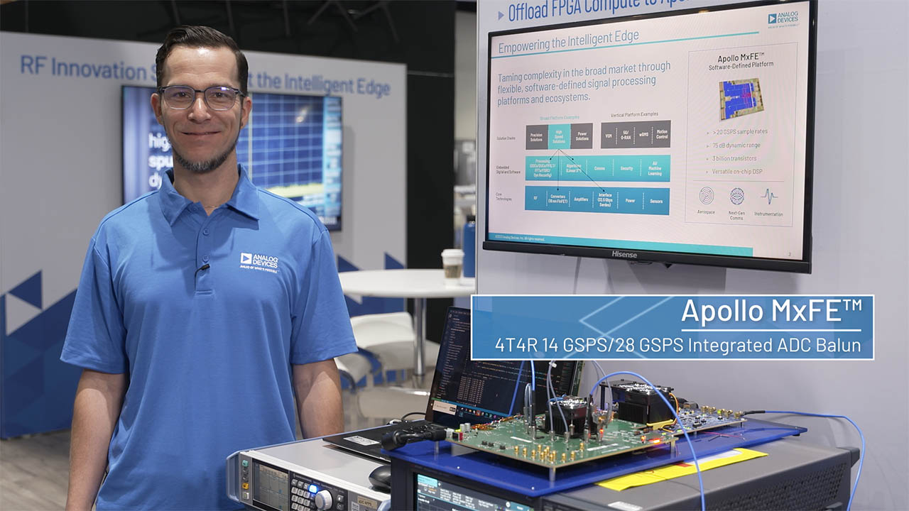
- 4 DACs and 4 ADCs (4D4A)
- Usable RF Analog bandwidth up to 18 GHz
- Maximum DAC/ADC sample rate up to 28 GSPS/20 GSPS
- DAC to ADC sample rate ratios of 1 and 2
- Clocking
- On-chip PLL (7 GHz to 14 GHz)
- External RFCLK input up to 20 GHz
- Multichip synchronization via subclass1
- Single-ended (SE) or differential (DIFF) ADC inputs
- Two separate versions, both 50 Ω input impedance
- Single-ended version with on-chip wide bandwidth balun
- Differential ADC AC performance at 20 GSPS
- Full-scale input voltage: 500 mV p-p/−2 dBm
- Noise density: −150 dBFS/Hz at −20 dBFS at 2 GHz
- HD2/HD3: −65 dBFS/−70 dBFS at −7 dBFS at 2 GHz
- IMD3: −75 dBFS at – 13 dBFS/tone at 2 GHz
- DAC AC performance at 28 GSPS
- Full-scale output power: −2.1 dBm at 2 GHz
- IMD3: −75 dBc at – 13 dBFS/tone at 2 GHz to 10 GHz
- NSD (shuffling disabled): −164 dBFS/Hz at 0 dBFS at 2 GHz
- Versatile digital features
- Supports real or complex digital data (8-, 12-, 16-bit)
- Configurable DDC and DUC
- 8 fine complex DUCs and 4 coarse complex DUCs
- 8 fine complex DDCs and 4 coarse complex DDCs
- Option to bypass fine and coarse DUC/DDC
- DUC/DDC alias rejection
- 85 dB for interpolation filters
- 100 dB for decimation filters
- Fractional sample rate converter (FSRC)
- Programmable FIR filters for transmit/receive
- Multiple loopback (ADC to DAC) supported
- ~45 ns without DSP path
- Dynamic configuration through SPI/HSCI/GPIO
- Spectrum sniffer/monitor
- Interfaces
- SPI
- High-Speed Control Interface (HSCI)
- JESD204B/JESD204C: 20 Gbps/32.5 Gbps
- 24 lanes for Rx, 24 lanes for Tx
- Receive AGC support
- Fast detect with low latency for fast AGC control
- Signal monitor for slow AGC control
- Auxiliary features
- Power amplifier downstream protection circuitry
- On-chip temperature monitoring unit
- TDD power savings option
- Total power consumption range dependent on device configuration: 20 W to 30 W
- 24 mm × 26 mm, 899-ball BGA with 0.8 mm pitch
- Operating junction temperature (TJ): −40°C to +110°C
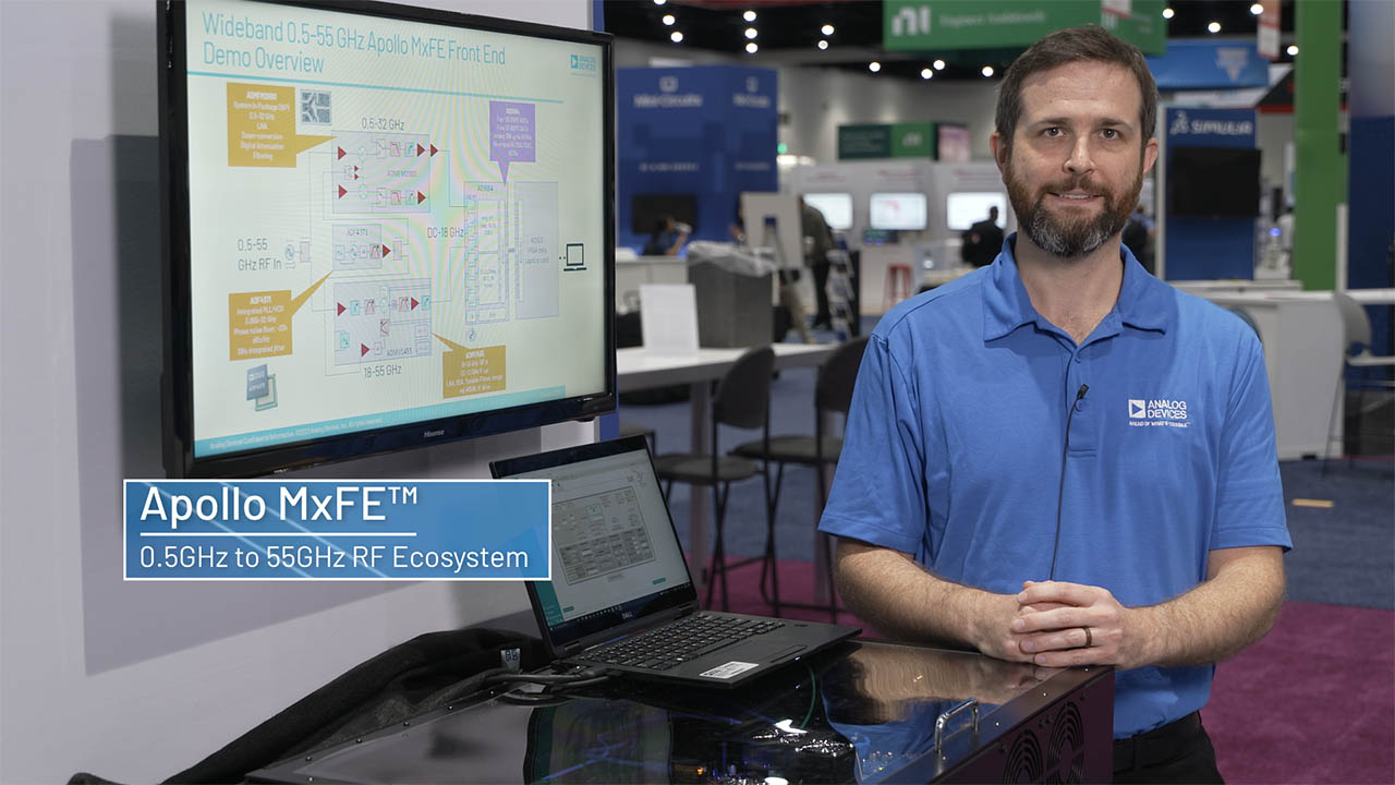
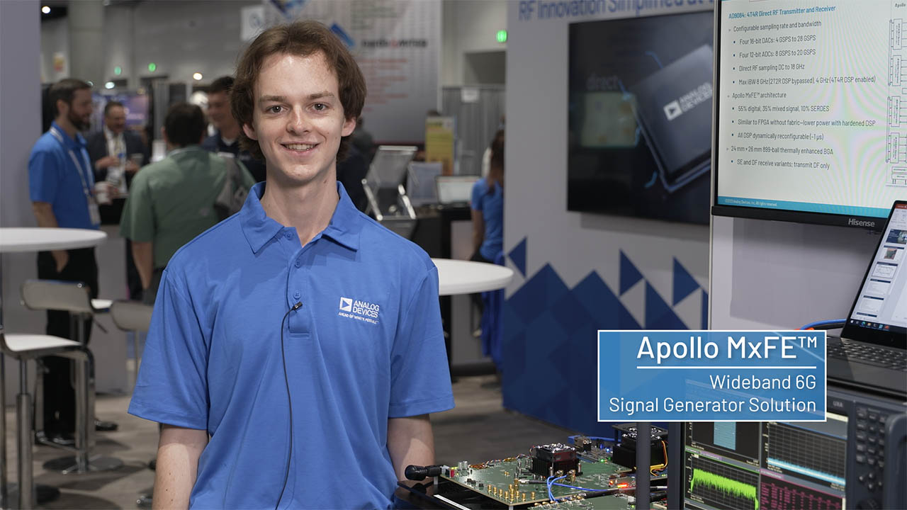
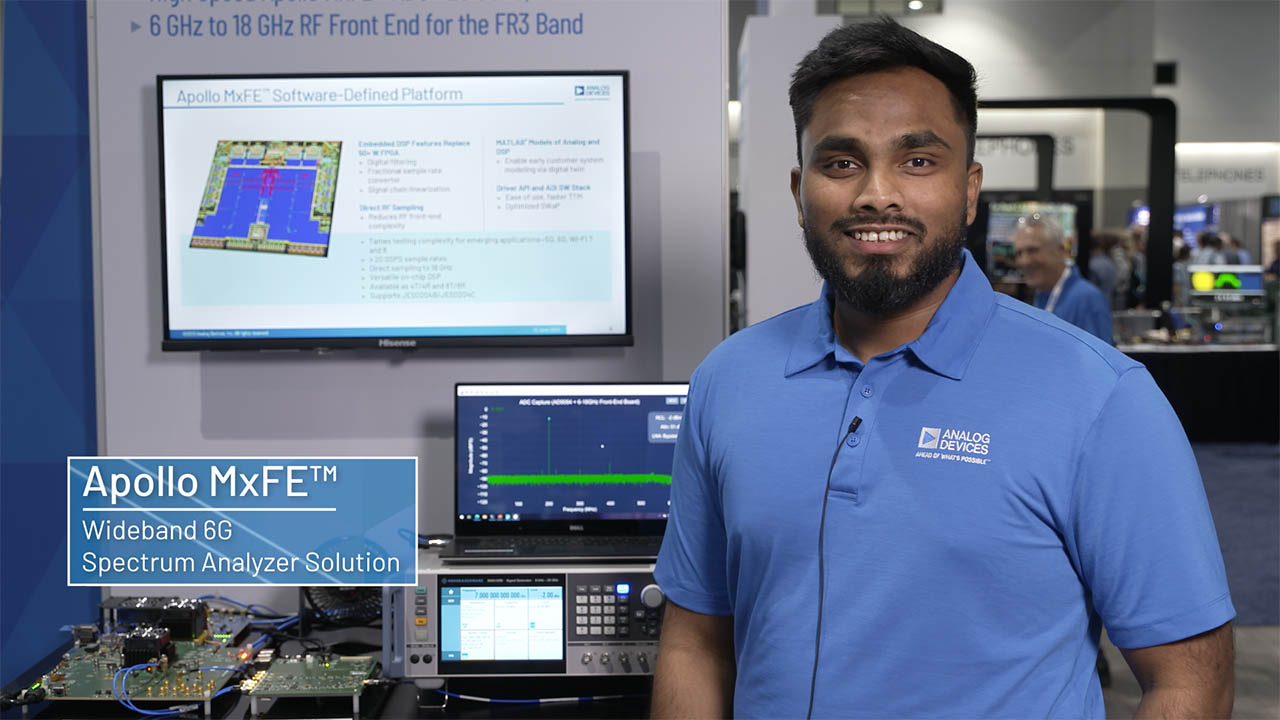
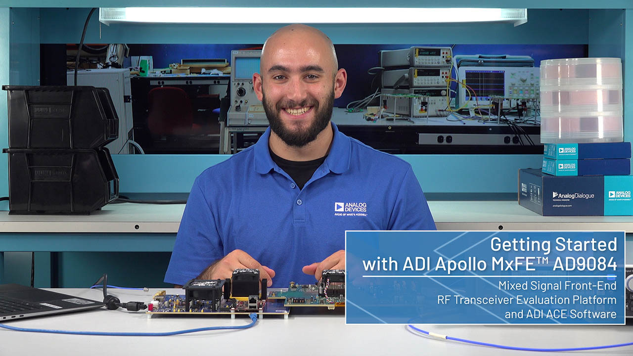
The Apollo mixed signal front-end (MxFE®) is a highly integrated device with a 16-bit, 28 GSPS maximum sample rate, RF digital-to-analog converter (DAC) core, and 12-bit, 20 GSPS maximum sample rate, RF analog-to-digital converter (ADC) core. The AD9084 supports four transmit channels and four receive channels. The AD9084 is well suited for applications requiring both wideband ADCs and DACs to process signal(s) having wide instantaneous bandwidth. The device features a 48 lane, 32.5 Gbps JESD204C or 20 Gbps JESD204B data transceiver port, an on-chip clock multiplier, and a digital signal processing (DSP) capability targeted at either wideband or multiband, direct to RF applications. The AD9084 also features a bypass mode that allows the full bandwidth capability of the ADC and/or DAC cores to bypass the DSP datapaths. The device also features low latency loopback and frequency hopping modes targeted at phased array radar systems and electronic warfare applications.
The AD9084 is available in a 24 mm x 26 mm, 899-ball BGA and operates within the –40°C to +110°C junction temperature range. For additional information, contact ApolloSupport@analog.com.
APPLICATIONS
- Radar and communications
- L/S/C/X/Ku band radar and electronic warfare
- Phase array system
- Broadband communications systems
- Electronic test and measurement systems
- Satellite communications
- Microwave point-to-point, X-band and 5G mmWave
Thank you for showing interest in Apollo MxFE™ and our upcoming AD9084/AD9088 product release! Subscribe to stay on top of Apollo news, TODAY!
参考资料
数据手册 1
技术文章 6
视频 8


这是最新版本的数据手册
评估套件


ADS10-V1EBZ Evaluation Board
资料
最新评论
需要发起讨论吗? 没有关于 ad9084的相关讨论?是否需要发起讨论?
在EngineerZone®上发起讨论