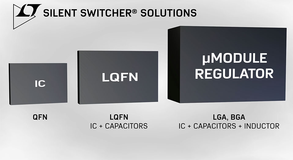
LTM8074

RECOMMENDED FOR NEW DESIGNS

40VIN, 1.2A Silent Switcher µModule Regulator

Part Models
3
1ku List Price
Starting From $4.50
Viewing:

Part Details

  • Low Noise Silent Switcher® Architecture
  • CISPR 22 Class B Compliance
  • Wide Input Voltage Range: 3.2V to 40V
  • Wide Output Voltage Range: 0.8V to 12V
  • 1.2A Continuous Output Current at 24VIN, 5VOUT, TA = 85°C
  • 1.75A Peak Output Current at 3.3VOUT
  • Selectable Switching Frequency: 200kHz to 2.2MHz
  • External Synchronization
  • Configurable as an Inverter
  • 4mm × 4mm × 1.82mm BGA Package
LTM8074
40VIN, 1.2A Silent Switcher µModule Regulator
LTM8074 Application Circuit LTM8074 Performance Graph LTM8074 Pin Configuration
Add to myAnalog

Add product to the Products section of myAnalog (to receive notifications), to an existing project or to a new project.

Create New Project
Ask a Question

Documentation

Learn More
Add to myAnalog

Add product to the Products section of myAnalog (to receive notifications), to an existing project or to a new project.

Create New Project

Tools & Simulations

LTspice

LTspice® is a powerful, fast and free simulation software, schematic capture and waveform viewer with enhancements and models for improving the simulation of analog circuits.

LTpowerCAD

LTpowerCAD® is a power supply design program which selects power stage components, provides detailed power efficiency, shows quick loop Bode plot stability and load transient analysis, and can export to LTspice for simulation.


Evaluation Kits

eval board
DC2753A

LTM8074 1.2A Step-Down Silent Switcher µModule Regulator

Product Details

Demonstration circuit 2753A features the LTM8074EY µModule regulator, a tiny high performance high efficiency step-down regulator with Silent Switcher® architecture. DC2753A has an operating input voltage range of 3.4V to 40V and is able to provide an output current of up to 1.2A. The output voltage can be programmed from 0.78V up to 15V. The LTM8074EY is a complete DC/DC point of load regulator in a thermally enhanced 4mm × 4mm × 1.82mm BGA package requiring only a few input and output capacitors.

The radiated EMI performances of the board (with EMI filter) are shown in Figure 6 and Figure 7. The demo board also has a conducted EMI filter installed. To use the conducted EMI filter, the input should be tied to VEMI, not VIN. An inductor L2, which is a 0Ω jumper on the board by default now, can be added in the EMI filter to further reduce the conducted emission.

The LTM8074 data sheet must be read in conjunction with this demo manual for working on or modifying DC2753A.

DC2753A
LTM8074 1.2A Step-Down Silent Switcher µModule Regulator
DC2753A Demo Board

Reference Designs

Figure 1. CN0585 Simplified Block Diagram
CN0585 Circuits from the lab

Quad Channel, Low Latency, Data Acquisition and Signal Generation Module

Features and Benefits

  • 4 Analog Input Channels with Configurable Voltage Ranges
  • 4 Analog Output Channels with Configurable Voltage Ranges
  • 200 ns Latency between ADC Measurement and DAC Settling
  • Analog Front End Interface Connector
  • Modeling and Simulation Compatible with MATLAB and Python
  • FMC Connector Interface to FPGA
CN0585
Quad Channel, Low Latency, Data Acquisition and Signal Generation Module
Figure 1. CN0585 Simplified Block Diagram
EVAL-CN0585-FMCZ Angle View
EVAL-CN0585-FMCZ Bottom View
EVAL-CN0585-FMCZ Top View

Latest Discussions

Recently Viewed