CN0273


Overview
Design Resources
Design & Integration File
- Schematic
- Bill of Materials
- Gerber Files
- PADS Files
- Assembly Drawing
Evaluation Hardware
Part Numbers with "Z" indicate RoHS Compliance. Boards checked are needed to evaluate this circuit.
- EVAL-CN0273-EB1Z ($70.62) High Speed FET Input Instrumentation Amplifier with Low Input Bias Current and High AC Common-Mode Rejection
Features & Benefits
- FET input instrumentation amplifier
- High bandwidth
- Small PCB footprint
Markets and Technologies
Parts Used
Documentation & Resources
-
MT-068: Difference and Current Sense Amplifiers5/13/2016PDF244 kB
-
MT-101: Decoupling Techniques2/14/2015PDF954 kB
-
MT-061: Instrumentation Amplifier (In-Amp) Basics2/14/2015PDF125 kB
-
MT-031: Grounding Data Converters and Solving the Mystery of "AGND" and "DGND"3/20/2009PDF144 kB
-
MT-064: In-Amp DC Error Sources2/3/2009PDF97 kB
-
MT-063: Basic Three Op Amp In-Amp Configuration2/3/2009PDF68 kB
Circuit Function & Benefits
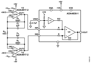
The circuit shown in Figure 1 is a high speed FET input, gain of- 5 instrumentation amplifier (in-amp) with a wide bandwidth (35 MHz) and excellent ac common-mode rejection, CMR, (55 dB at 10 MHz). The circuit is ideal for applications where a high input impedance, fast in-amp is required, including RF, video, optical signal sensing, and high speed instrumentation. The high CMR and bandwidth also makes it ideal as a wideband differential line receiver.
Most discrete in-amps require expensive matched resistor networks to achieve high CMR; however, this circuit uses an integrated difference amplifier with on-chip matched resistors to improve performance, reduce cost, and minimize printed circuit board (PCB) layout area.
The composite in-amp circuit shown in Figure 1 has the following performance:
- Offset voltage: 4 mV maximum
- Input bias current: 2 pA typical
- Input common-mode voltage: −3.5 V to +2.2 V maximum
- Input differential voltage: ±3.5 V/G1 maximum, where G1 is the gain of the first stage
- Output voltage swing: 0.01 V to 4.75 V typical with 150 Ω load
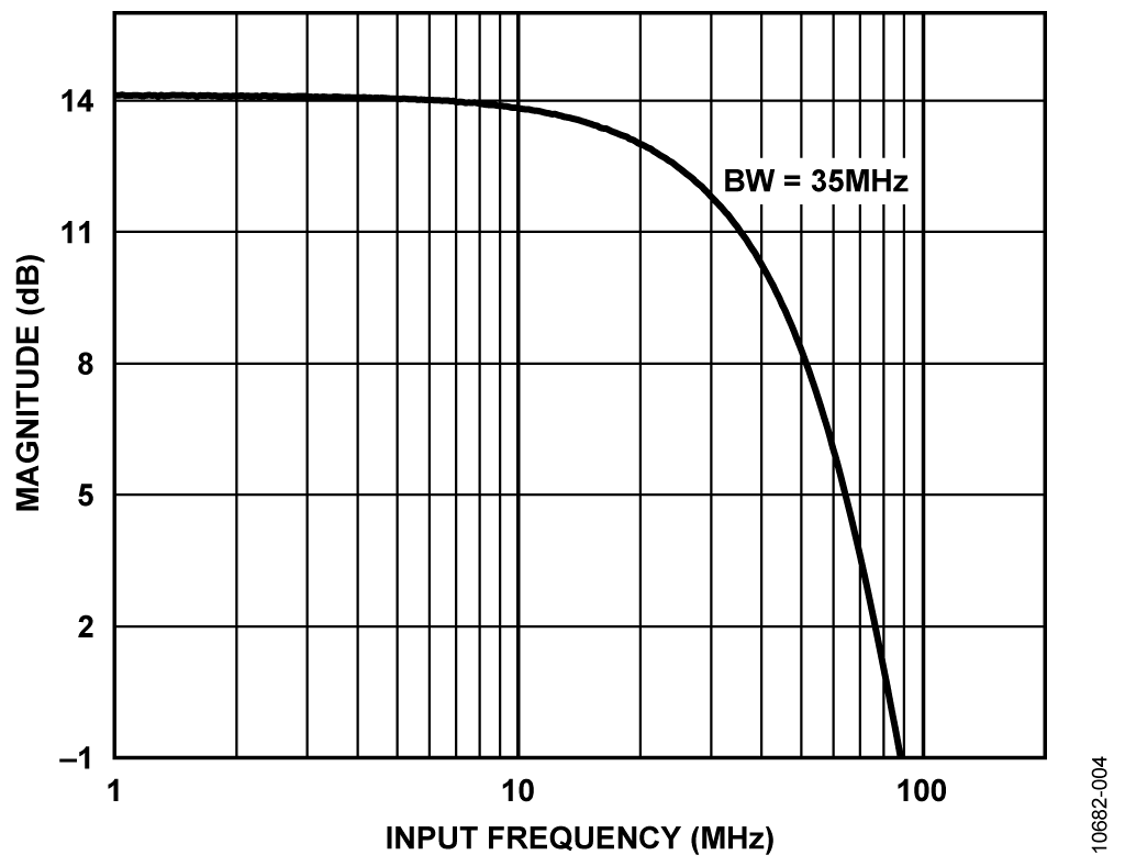
- Bandwidth (−3 dB): 35 MHz typical for G = 5
- Common-mode rejection: 55 dB at 10 MHz typical
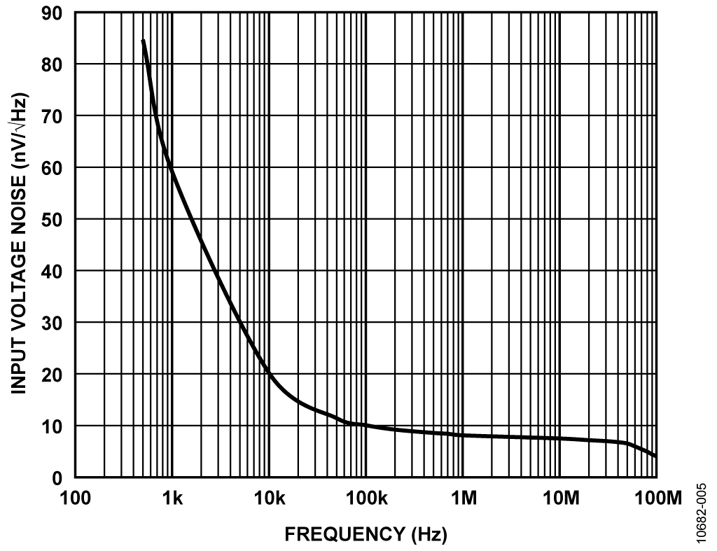
- Input voltage noise: 10 nV/√Hz at 100 kHz RTI typical
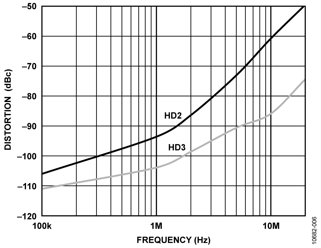
- Harmonic distortion: −60 dBc at 10 MHz, G = 5, VOUT = 1 V p-p, RL = 1 kΩ


Most fully integrated in-amps are fabricated on bipolar or complementary bipolar processes and are optimized for low frequency applications with high CMR at 50 Hz or 60 Hz. However, there is a growing need for wide bandwidth in-amps for video and RF systems to amplify high speed signals and provide common-mode rejection of unwanted high frequency signals.
When a very high speed, wide bandwidth in-amp is needed, one common approach is to use two discrete op amps with high input impedance to buffer and amplify the differential input signal in the first stage, and then configure a single amplifier as a difference amplifier in the second stage to provide a differential-to-single-ended conversion. This configuration is known generally as a 3-op-amp in-amp. This approach requires four relatively expensive precision-matched resistors for good CMR. Errors in matching produce errors at the final output.
The circuit shown in Figure 1 solves this problem by using the ADA4830-1 integrated high speed difference amplifier. The laser-trimmed thin film resistors are matched to very high precision, thereby eliminating the need for four relatively expensive precision-matched external resistors.
In addition, the use of the high speed, dual ADA4817-2 as the input stage amplifier allows the composite in-amp to provide a bandwidth as high as 80 MHz when the overall gain of the circuit is 2.5.
The use of the dual ADA4817-2 amplifiers in a single 4 mm × 4 mm LFCSP package and the integrated ADA4830-1 difference amplifier significantly reduces board space, thereby reducing design costs for large systems.
The circuit can be used in noisy environments because both the ADA4817-2 and ADA4830-1 offer low noise and excellent CMR performance at high frequencies.
Circuit Description
The circuit is based on the traditional 3-op-amp in-amp topology with two op amps for the input gain stage and a difference amplifier for the output stage. The circuit has as a gain of 5 and a bandwidth of 35 MHz.
FET Amplifier Input Gain Stage
The ADA4817-2 (dual) FastFET amplifiers are unity-gain stable, ultrahigh speed voltage feedback amplifiers with FET inputs. These amplifiers are fabricated on Analog Devices, Inc., proprietary eXtra Fast Complementary Bipolar (XFCB) process, which allows the amplifiers to achieve ultralow noise as well as very high input impedances and high speed, making it ideal for applications where high speed and high source impedances are required.
The ADA4817-2 op amps are configured so that they share the RG gain resistor. The circuit has a gain of 1 + 2RF/RG for the differential inputs. When the inputs are common-mode, there is no current flowing through the RG gain resistor. Thus, the circuit acts as a buffer for the common-mode inputs. The common-mode inputs are then effectively removed by the second stage difference amplifier.
The ADA4817-2 has a unity-gain bandwidth product, fu, of 410 MHz. Its close-looped bandwidth can be approximated by

where G1 is the gain of the first stage.
For this circuit, with a first stage closed-loop gain of 10, the −3 dB bandwidth is estimated to be 41 MHz. This is very close to the tested bandwidth of 35 MHz.
Parasitic capacitance in the PCB boards and capacitive loads can cause the first gain stage to oscillate. This issue can be alleviated by using low value feedback resistors, and the use of feedback capacitance.
For this circuit, a feedback resistor of 200 Ω was chosen. The feedback capacitor, CF, was 2 pF for the best bandwidth flatness.
Difference Amplifier and CMR
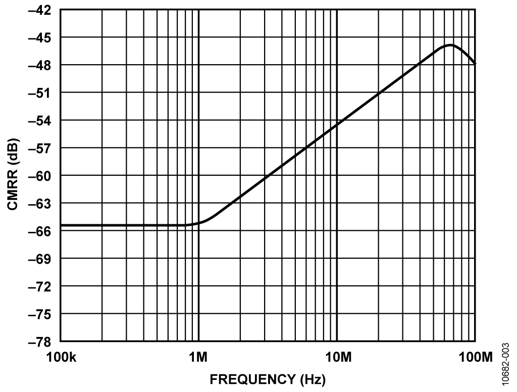
The ADA4830-1 is high speed difference amplifier with a wide common-mode voltage range. It combines high speed and precision. It offers a fixed gain of 0.5 V/V, and −3 dB bandwidth of 84 MHz. The on-chip, laser-trimmed resistors yield a typical CMR of 55 dB at 10MHz. CMR is a very important specification for in-amps and depends mostly on the ratio matching of the four resistors used in the second stage difference amplifier, as is shown in Figure 2.


In general, the worst-case CMR is given by

where Kr is the individual resistor tolerance in fractional form. The previous equation shows that the worst-case CMR for four resistors with the same nominal values (1% tolerance) is 34 dB. Instead of using discrete resistors, this circuit uses a monolithic ADA4830-1 difference amplifier with on-chip, laser-trimmed thin film resistors, thereby providing excellent CMR and saving PCB space. The CMR is 65 dB at dc and 55 dB at 10 MHz.
Differential and Common-Mode Voltage Considerations
To maximize the input voltage range and simplify the power supply requirements, the first stage of the circuit operates on ±5 V, whereas the second stage operates at +5 V. The maximum differential input range is determined by the output swing of the ADA4817-2. With a ±5 V supply, the ADA4817-2 has an output swing of ±3.5 V.
Therefore, the maximum allowable differential input is ±3.5 V/G1, where G1 is the gain of the first stage. Note that there is a tradeoff between the maximum allowable differential input and the closed loop gain of the first stage.
The next step is to analyze the common-mode voltage restrictions. The common-mode voltage at the input to the ADA4817-2 must fall between −VS to +VS − 1.8 V, or −5 V to +2.2 V for ±5 V supplies. The output swing of the ADA4817-2 is limited to ±3.5 V when operating on ±5 V supplies (refer to the ADA4817-2 data sheet). The negative input common-mode voltage of the circuit is therefore limited to −3.5 V by the output swing of the ADA4817-2.
Therefore, the allowable input common-mode range for the composite circuit is −3.5 V to +2.2 V.
To achieve high performance from this circuit, excellent layout, grounding, and decoupling techniques must be applied. See MT-031 Tutorial, MT-101 Tutorial, and the A Practical Guide to High-Speed Printed-Circuit-Board Layout article for more detailed information regarding PCB layout. In addition, there are layout guidelines within the ADA4817-2 datasheet and the ADA4830-1 data sheet.
Circuit Performance
The four most important parameters of this composite circuit, CMR, −3 dB bandwidth, input referred noise, and harmonic distortion, are tested, and the results are shown in Figure 3 to Figure 6.
Figure 3 shows that the CMR of the composite circuit is −65 dB at dc and −55 dB at 10 MHz. Figure 4 shows that the bandwidth is 35 MHz at a gain of 5 and an output load of 100 Ω. Figure 5 shows that the composite circuit only has 10 nV/√Hz input referred noise at 100 kHz and a flatband noise of 8 nV/√Hz at higher frequencies. Figure 6 shows that the circuit has a THD of 60 dBc at10 MHz, with VOUT =1 V p-p and RL = 1 kΩ.


Common Variations
The overall gain of this circuit can be easily configured by the value of the gain resistor, RG, shown in Figure 1. Note that with a larger overall gain, the bandwidth of this circuit decreases.
The difference amplifier at the second stage can be replaced by the AD8274 in lower speed applications. The AD8274 difference amplifier offers a fixed gain of 2. Therefore, a larger overall gain can be achieved.
To increase the input common-mode and differential range, a rail-to-rail high speed FET input amplifier, such as the AD8065/AD8066 that operates on ±12 V supplies and has a unity-gain bandwidth of 145 MHz, can be used.
Circuit Evaluation & Test
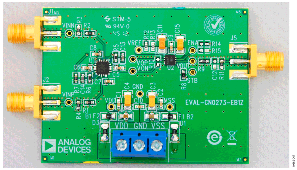
The circuit can be easily evaluated using a signal generator and an oscilloscope. The board is tested with traditional amplifier test methods using a network analyzer. For complete schematics and PCB layout, refer to the CN0273-Design Support package. A photo of the board is shown in Figure 7.
Note that the CMRR data in Figure 3 was taken for a differential input voltage of 0 V. The bandwidth data in Figure 4 and the distortion data in Figure 6 were taken using a balanced differential drive source with a common-mode voltage of 0 V.