CN0354


Overview
Design Resources
Design & Integration File
- Schematic
- Bill of Materials
- Gerber Files
- PADS Files
- Assembly Drawing
Evaluation Hardware
Part Numbers with "Z" indicate RoHS Compliance. Boards checked are needed to evaluate this circuit.
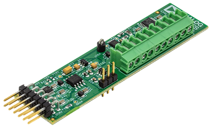
- EVAL-CN0354-PMDZ ($42.80) Low Power Multichannel Thermocouple Measurement System with Cold Junction Compensation
- EVAL-SDP-CB1Z ($116.52) Eval Control Board
- SDP-PMD-IB1Z ($64.74) PMOD to SDP Interposer Board
Device Drivers
Software such as C code and/or FPGA code, used to communicate with component's digital interface.
Markets and Technologies
Parts Used
Documentation & Resources
-
CN-0354 Software User Guide10/16/2018WIKI
Circuit Function & Benefits
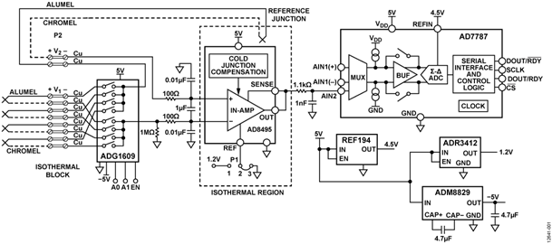
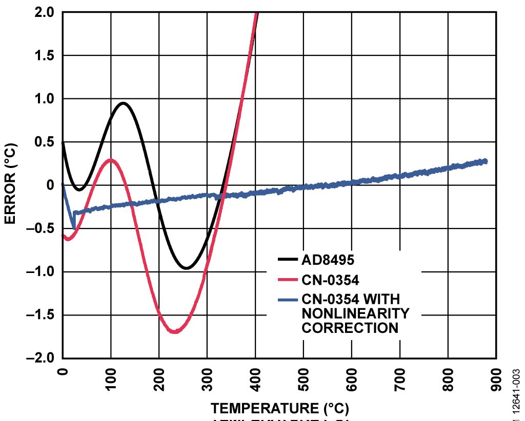
The circuit shown in Figure 1 is a flexible, 4-channel, low power thermocouple measurement circuit with an overall power consumption of less than 8 mW. The circuit has a multiplexed front end, followed by an instrumentation amplifier that performs cold junction compensation (0°C to 50°C) and converts the thermocouple output to a voltage with a precise scale factor of 5 mV/°C. The error is less than 2°C, over a measurement range of −25°C to +400°C, and is primarily due to the thermocouple nonlinearity. A nonlinearity correction algorithm reduces the error to less than 0.5°C over a 900°C measurement range. Noise free resolution is less than 0.1°C.
The signal is then digitized by a 24-bit Σ-Δ ADC, and the digital value is provided on an SPI serial interface. With the PMOD form factor for rapid prototyping, the design requires minimal PC board area and is ideal for applications that require precise thermocouple temperature measurements.


Circuit Description
The four thermocouple inputs to the circuit are terminated at the isothermal block, P2. The ADG1609 complementary metal oxide semiconductor (CMOS) analog multiplexer switches the four thermocouple channels to a single signal conditioning block to handle the four thermocouple inputs. The switches exhibit a break-before-make switching action and an inherent low charge injection to minimize transients when switching between channels.
The thermocouple voltage generated at the output of the isothermal block is proportional to the difference between the temperature at the measurement thermocouple and the temperature of the isothermal block (cold junction).
The signal is amplified by the AD8495, a precision instrumentation amplifier that is laser trimmed to provide a precise 5°mV/°C output for a K type thermocouple. The AD8495 also provides cold junction compensation over a range of 0°C to 50°C.
The fifth thermocouple, shown in Figure 1, is added to cancel the voltage generated by any temperature differential that exists between the isothermal block and the AD8495 cold junction compensation circuit. With the multiplexer enabled, the constantan (alumel) copper junction, formed by the thermocouple connection at the isothermal block, is in series with a copper constantan (alumel) junction, formed by the reference thermocouple connection. This series combination contributes equal but opposite voltages because the block is isothermal. In this condition, the AD8495 internal cold junction compensation compensates for the reference junction at the IC, which must remain between 0°C and 50°C. Therefore, the fifth thermocouple connection option eliminates the requirement of mounting the AD8495 directly on the isothermal block, as is normally the case. If the fifth thermocouple is not connected, pins 5 and 6 of P2 should be connected with a short wire. Because of the proximity of P2 to the AD8495 the error produced will be minimal.
The output of the AD8495 is filtered by the 1.1 kΩ/1 nF single-pole filter that has a −3 dB cutoff frequency of 145 kHz. This filter minimizes broadband noise at the AD7787 ADC input.
The AD7787 is a 24-bit, low noise, low power Σ-Δ ADC for low frequency measurement applications, such as thermocouple measurement systems. Its internal clock eliminates the need for an external clock and makes the output data rate user configurable, which can reduce current consumption because it functions at a lower internal clock frequency. It contains a Σ-Δ ADC with one differential input and one single-ended input, either of which can be buffered or unbuffered after passing through the multiplexer.
The AD7787 operates from an internal clock. Therefore, the user does not have to supply a clock source to the device. The output data rate from the device is software programmable and can be varied from 9.5 Hz to 120 Hz, with the rms noise equal to 1.1 μV at the lower update rate. The AD7787 operates at an update rate of 9.5 Hz in this circuit. The internal clock frequency can be divided by a factor of 2, 4, or 8, which leads to a reduction in the current consumption. The update rate, cutoff frequency, and settling time all scale with the clock frequency.
The AD7787 operates with a power supply from 2.5 V to 5.25 V. When operating from the 3 V supply, the power dissipation for the device is 225 μW maximum. It is packaged in a 10-lead MSOP.
Thermocouple Signal Conditioning
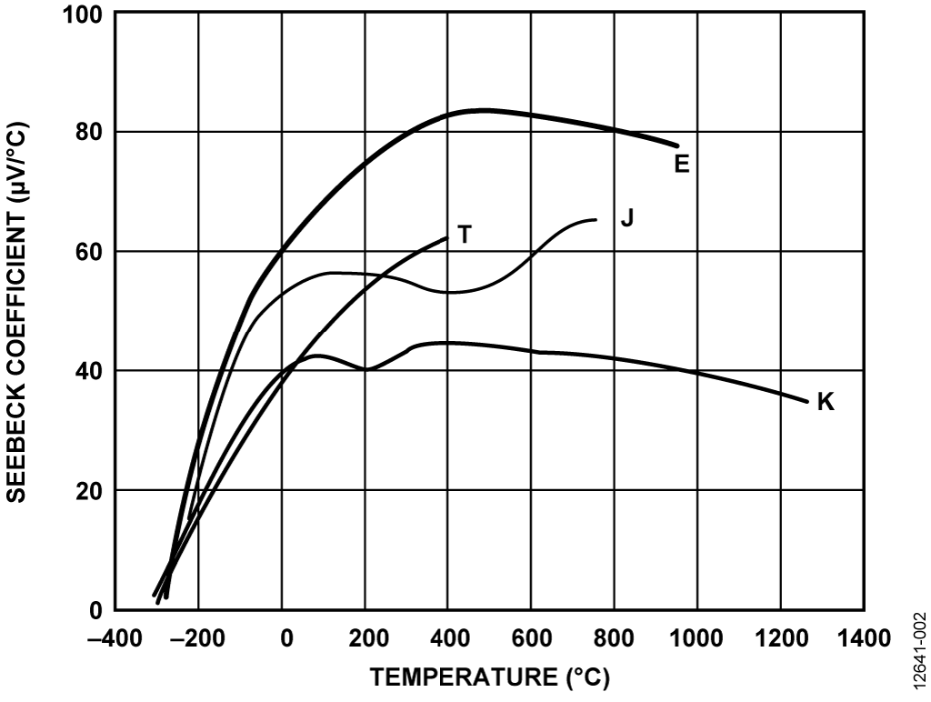
Thermocouples are used in temperature measurement requiring high temperature ranges. They are preferred over resistance temperature detectors (RTDs) for this reason, as well as for their lower cost. However, thermocouples are nonlinear, which means that the voltage generated by a thermocouplechanges at different rates and at different temperatures. For example, a J type thermocouple changes by 52 μV/°C at 25°C and by 55 μV/°C at 150°C. K type thermocouples tend to be more linear, at approximately 41 μV/°C, when temperatures are above 0°C. The voltage response of a thermocouple to a temperature gradient is generally described by a polynomial of greater than the sixth-order.
Figure 2 shows the Seebeck coefficient of the different types of thermocouples over their operating temperature ranges. Figure 2 shows that the K type thermocouple has the widest temperature range and can measure temperatures up to 1250°C.

Due to the nonlinear characteristic of thermocouples, complex signal processing and signal conditioning are required to obtain a precise temperature reading, and the AD8495 provides an ideal solution.
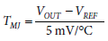
The AD8495 is trimmed to provide cold junction compensation over a reference junction range of 0°C to 50°C and provides a linear 5 mV/°C transfer function. Over a measurement range of −25°C to +400°C, the maximum output error is ±2°C. To calculate the output voltage, use the following equation:
The AD8495 operates on a single 5 V supply in the circuit. Because of the PNP transistor input structure, the input voltage can be as low as −200 mV, thereby allowing the measurement of negative temperatures. However, the output voltage must be offset in order to process negative temperatures, which is accomplished using the reference voltage input pin (REF).
With the REF pin grounded using the P1 jumper, the minimum temperature that the system can measure is 5°C. The P1 jumper also allows the REF pin bias voltage to connect to a 1.2 V ADR3412 reference, thereby allowing measurement temperatures as low as −235°C. The corresponding temperature range for either condition is specified in Table 1. In both cases, the temperature span is 875°C. It is important to drive the REF pin with a low impedance source, such as a voltage reference or a buffer amplifier, to prevent errors.
| REF Pin Voltage | Temperature Range |
| 0 V or Grounded | 5°C to 880°C |
| 1.2 V | -235°C to +640°C |
Open Thermocouple Detection
The AD8495 can detect an open or broken thermocouple. The inputs of the AD8495 are the bases of PNP transistors; therefore, the bias current always flows out of the inputs. If either input is open, the output goes to one of the supply rails. Connecting the negative input to ground through a 1 MΩ resistor causes the AD8495 output to rail high in an open thermocouple condition. In cases where any of the four channels are not used, short the inputs to prevent the AD8495 from railing to the positive supply if that channel is connected. The 1 MΩ resistor also provides a bias current return path to ground.
The AD8495 has a high common-mode rejection, thereby minimizing the common-mode noise picked up by long thermocouple leads. The high impedance inputs of the amplifier make it easy to add extra filtering for additional electromagnetic interference /radio frequency interference (EMI/RFI) protection.
Power Considerations
The circuit in Figure 1 is powered from a single 5 V supply that powers the ADG1609, the AD8495, the VDD pin of the AD7787, the REF194, the ADR3412, and the ADM8829.
The REF194 supplies the 4.5 V reference for the AD7787. The ADR3412 provides the 1.2 V optional offset voltage for the REF input of the AD8495. Jumper P1 allows the REF pin to be connected either to 1.2 V or to ground.
The ADM8829 switched capacitor voltage inverter provides the −5 V required by the ADG1609 multiplexer to accommodate negative temperatures.
Table 2 shows the current consumed by each device in the circuit, based on the data sheet specifications. The design consumes a maximum of 1.56 mA. Note that the maximum current consumption is due to the ADM8829 switched capacitor voltage inverter. This inverter can be eliminated if a negative supply is available to drive the VSS pin of the ADG1609, thereby reducing the total current to about 556 μA.
| Part Number | Maximum Current Consumption |
| AD8495 | 250 µA |
| AD7787 | 160 µA |
| ADG1609 | 1 µA |
| REF194 | 45 µA |
| ADR3412 | 100 µA |
| ADM8829 | 1000 µA |
Note that the total current is 1556 μA.
Test Results
The AD8495 has a maximum temperature error due to the thermocouple nonlinearity of ±2°C from −25°C to +400°C, for a reference junction temperature of 0°C to 50°C. Wider temperature ranges or better accuracy requires a linearity correction algorithm that can be implemented in the software. Nonlinearity correction is discussed in the AN-1087 Application Note, Thermocouple Linearization When Using the AD8494/AD8495/AD8496/AD8497. Figure 3 shows the linearity error of the circuit, with and without the correction algorithm implemented.

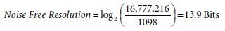
The noise of the system was tested in a controlled temperature environment to check the noise free code resolution of the system. Figure 4 shows the noise distribution, which spans approximately 1098 codes. For a 24-bit resolution and a span of 900°C, 1 LSB = 900°C/224 = 0.07°C resolution.
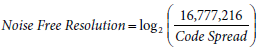

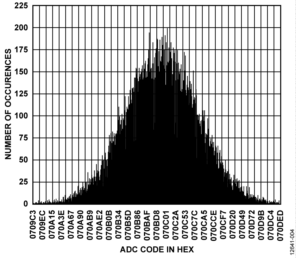
Calculate the noise free code resolution as follows:
Common Variations
The CN-0354 circuit was proven to work with good stability and accuracy with the devices selected for the design.
This design can also be implemented using the AD594/AD595, which are also single chip thermocouple, signal conditioning amplifiers, with an output of 10 mV/°C.
The AD8495 has other variants, such as the AD8494, the AD8496, and the AD8497, for different thermocouple types, different ambient temperature ranges, and different measurement temperature ranges, as shown in Table 3.
| Device | Thermocouple Type | Maximum Error | Ambient Temperature Range | Measurement Temperature Range |
| AD8494 | J | ±2°C | 0°C to 50°C | -35°C to +95°C |
| AD8495 | K | ±2°C | 0°C to 50°C | -25°C to +400°C |
| AD8496 | J | ±2°C | 25°C to 100°C | 55°C to 565°C |
| AD8497 | k | ±2°C | 25°C to 100°C | -25°C to +295°C |
Circuit Evaluation & Test
Equipment Required
The following information is needed:
- The EVAL-CN0354-PMDZ evaluation board
- The EVAL-SDP-CB1Z System Demonstration Platform
- The PMD-SDP-IB1Z, SDP-I-PMOD, interposer board
- Short piece of Type K thermocouple wire if additional temperature compensation is desired. Otherwise, connect a short wire between screw terminals 5 and 6 of P2.
- The CN0354 Evaluation Software
- 6 V wall wart power supply
- PC (Windows 32-bit or 64-bit)
Software Installation
The CN-0354 evaluation kit includes self installing software on a CD. The software is compatible with Windows® XP (SP2), Vista (32-bit and 64-bit), and Windows 7 (32-bit and 64-bit). If the setup file does not run automatically, run the setup.exe file from the CD. Install the evaluation software before connecting the evaluation board and the SDP board to the USB port of the PC to ensure that the evaluation system is correctly recognized when connected to the PC. The software allows full configuration of the serial interface. It is important that the configurations of the masters and the slaves match for proper operation.
Software operation is described in the CN-0354 Software User Guide.
Power Supply Requirements
The EVAL-CN0354-PMDZ evaluation board must be powered by a 5 V power supply. It is recommended that the supply provide at least 2 mA. If powered directly from the PMD-SDP-IB1Z interposer board, ensure that the supply is well filtered and free of digital noise.
Test Setup Functional Diagram
A functional diagram of the test setup is shown in Figure 5, and a photo of the EVAL-CN0354-PMDZ board is shown in Figure 6.

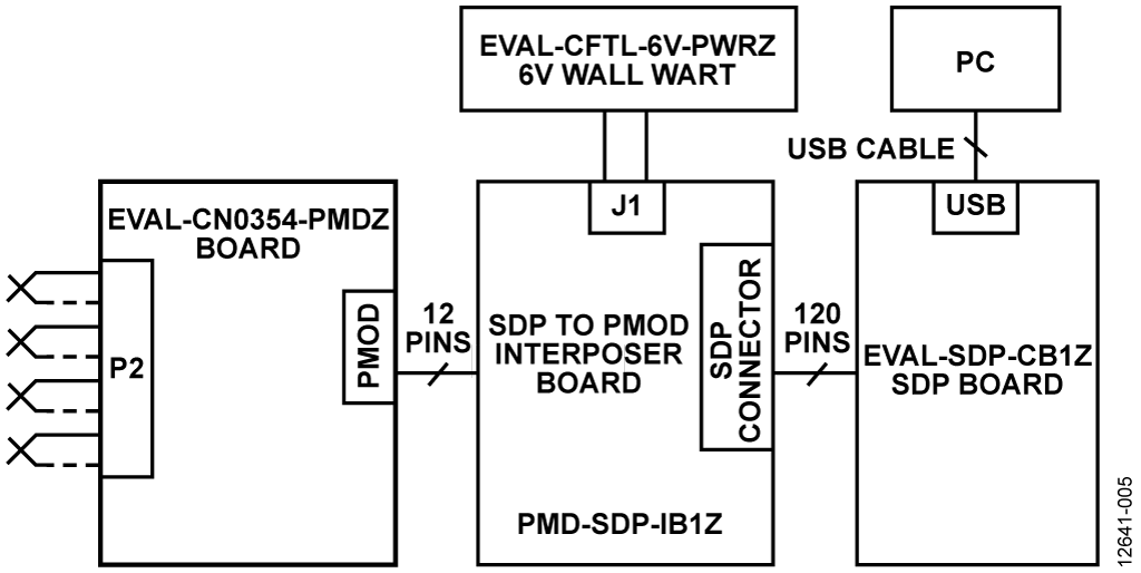
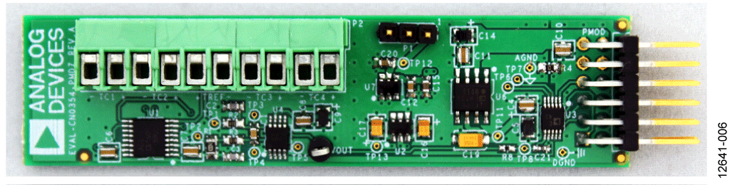
Figure 6. EVAL-CN0354-PMDZ Evaluation Board