MAXREFDES71
MAXREFDES71: 2-Channel Analog Input/Analog Output with Transformer Driven Power


Overview
設計リソース
説明
Advanced manufacturing, custom production and cost pressures continue to drive factories to higher speed performance and increased flexibility. To meet the requirements of a ‘no compromises’ factory environment, the MAXREFDES71 subsystem reference design provides two high-speed, high-accuracy, 400ksps, 16-bit analog input channels and output channels. All input and output channels support ±10V and ±20mA signals plus 20% margin, providing flexibility for low- and high-speed systems using either voltage or current signals.
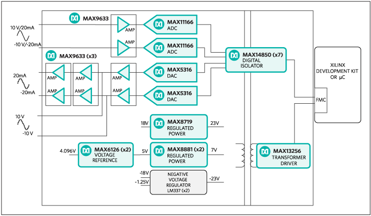
The MAXREFDES71 design utilizes four dual fast-settling high-voltage op amps (MAX9633); two 16-bit 500ksps ADCs (MAX11166); two low-noise, fast-settling precision 16-bit DACs (MAX5316); two ultra-high precision 4.096V voltage references (MAX6126); seven high-speed digital isolators (MAX14850); an H-bridge transformer driver for isolated supplies (MAX13256); and regulated +18V, -18V, +5V, and -1.25V power rails (MAX8719, MAX8881). By using high-accuracy and high-speed components, this subsystem performs well in both process control applications, such as sensor inputs, and control applications, such as servo drives, resolvers, and encoders.
機能と利点
Applications
- Industrial control automation
- Servo drive
Competitive Advantages
- High speed
- High accuracy
- Low noise
Features
- Two independent analog inputs
- Two independent analog outputs
- Isolated power and data
- High-speed 400ksps analog input sampling rate
- High-accuracy 16-bit resolution
- Voltage output settles to within 2 LSB in 17µs
- Current output settles to within 2 LSB in 77µs
- Device drivers
- Example C source code
- Configuration files for ZedBoard™ platform
- FMC-compatible
Details Section


Documentation & Resources
-
MAXREFDES71 Design FIles2021/02/17ZIP26 M
-
UG-5866: MAXREFDES71# ZedBoard Quick Start Guide2014/06/27PDF2M
Support & Training
Search our knowledge base for answers to your technical questions. Our dedicated team of Applications Engineers are also available to answer your technical questions.