Precision DAC and Watchdog Improve Analog Output Safety
要約
Using a DAC and a microprocessor supervisor, the system safety can be improved in industrial controllers, programmable-logic controllers (PLC), and data-acquisition systems. The analog output is set to zero-scale (or pin-programmable midscale) when a microprocessor failure, optocoupler failure, or undervoltage condition occurs. A simple application is shown on how to implement this function.
A similar version of this article appeared on Hearst Electronic Products, December 18, 2012.
Introduction
The need for safe states in industrial applications is critical when system-level failures occur. A feature-rich precision digital-to-analog converter (DAC) and microprocessor (µP) supervisory circuit with watchdog timer can be used to assure that analog outputs default to a known midscale or zero-scale level.
Circuit Operation
Common analog-output control signals used in industrial controllers, programmable-logic controllers (PLCs), and data-acquisition systems (DAS) include voltage outputs such as 0 to 5V, 0 to 10V, ±5V, ±10V, and 4–20mA current loop. To ensure safety integrity, the analog-output control signal should default to a known midscale or zero-scale safe state in response to a µP or system failure. For additional safety, analog output modules often employ optocouplers to provide galvanic isolation between the µP and analog output signals.
Requirements for analog output safety and reliability are met by the Figure 1 circuit. When a µP failure, optocoupler failure, or undervoltage condition occurs, the supervisory circuit (U3, the MAX6303) sets the 12-bit DAC (U2, the MAX5120) analog output to mid-scale, which in turn sets VOUT to 0V safe-state output. This circuit also improves mean time between failure (MTBF) by reducing the number of I/O pins at the µP and by eliminating an optocoupler.
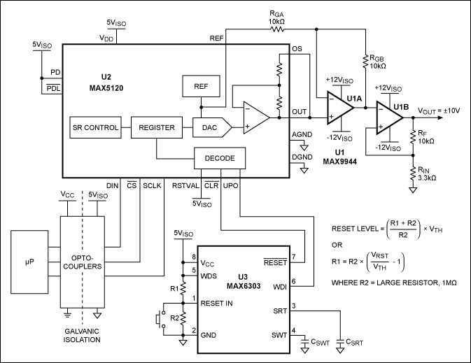
Figure 1. When a failure occurs in the supply voltage, optocouplers, or µP operation, this DAC (U2) and µP supervisor (U3) together generate a user-programmed, safe-state default output (VOUT).
Three DAC features enable the circuit to meet the safety-critical functions: an asynchronous reset input (active-low CLR), a user-selectable reset-value input (RSTVAL), and a user-programmable output (UPO). These built-in features also eliminate the need for an optocoupler, reduce the number of I/O pins at the µP, and eliminate external discrete circuitry. The µP supervisor includes a resistor-programmable reset input threshold, a capacitor-programmable watchdog timer, and a reset timeout period.
Here is how the circuit works. As DAC codes range from 000hex to FFFhex, the analog output voltage (VOUT) ranges from -10V to +10V. Op amp U1A (MAX9944) is offset by the DAC's internal 10ppm/°C precision bandgap reference; output op amp U1B (MAX9944) is configured as a buffer with a gain of 4.
Output voltage for the circuit is calculated as:
VOUT = VREF × (G × NB/4096 - 1) × (RF/RIN + 1)
Where NB is the numeric value of the DAC's binary code; VREF is the internal reference voltage; G is the gain of U1A; and RF/RIN is U1B's gain-resistor ratio.
Microprocessor supervisor U3 monitors the isolated supply voltage (VISO) through its VCC pin. It also monitors µP activity at the WDI pin with UPO and generates a reset output command through active-low RESET. A resistor-divider at RESET IN (U3 pin 1) determines the reset-level voltage threshold (VTH). Similarly, the reset timeout period (tRP) and watchdog timeout period (tWD) are determined by capacitor values at SRT and SWT. Connect WDS to VCC to enter extended mode, lengthening tWD by a factor of 500. The following equations calculate values needed in the circuit:
VRST = VTH(R1 + R2)/R2
Where VTH = 1.22V and VRST is the adjustable reset threshold voltage:
CSRT = tRP/2.67
Where CSRT is in pF and tRP is in µs; CSWT is in pF and tWD is in µs. Therefore:
CSWT = tWD/(500 × 2.67)
If VCC fails or if the µP cannot toggle WDI via UPO, then U3 asserts the active-low RESET output which resets U2 through its CLR input. This action resets U2's output to the condition set by RSTVAL (to midscale in this case, which produces 0V at VOUT). In normal operation the µP must update U2 at intervals less than the programmed watchdog timeout period (tWD). In this manner the UPO output routinely toggles WDI, meaning that UPO "kicks the dog" at WDI. Note that after the reset timeout period (tRP), active-low RESET releases CLR but the DAC output remains at midscale until updated.
The switch between U3's RESET IN and GND terminals allows the user to command an emergency shutdown. Other devices to consider for the watchdog function are the MAX6316 series and the MAX6369 series, both of which offer fixed timeout periods and are available in SOT23 packages. Also, the DAC's unipolar and bipolar modes allow it to produce all common analog-output control signals.
Conclusion
Improvements to safety integrity can be realized with the special features of a precision DAC and watchdog timer µP supervisor. Together these devices can provide safe state operating conditions for the analog outputs used in many industrial-controller applications.