Measuring the Output Jitter of the MAX999 Comparator
要約
In some applications where a high-speed comparator like the MAX999 is used to square an input sinusoidal signal to generate an output clock, it may be important to know the jitter of the generated clock. This application note reviews basic jitter theory and then presents a circuit that can be used to extrapolate the jitter of the MAX999. The jitter measurement is then correlated to the input-referred voltage noise of the comparator.
Overview of Basic Jitter Theory1
The Fibre Channel Standard defines jitter as "the deviation from the ideal timing of an event." Fundamentally, jitter describes the timing error of a system, and it comprises two basic types: deterministic jitter and random jitter.
Deterministic jitter (DJ) is defined as jitter with a non-Gaussian probability density function. Deterministic jitter is always bounded in time and has specific causes: duty-cycle distortion (due to timing differences between rising and falling edges), EMI, crosstalk, and grounding and power-supply problems. Deterministic jitter is typically characterized by its bounded peak-to-peak value.
Random jitter (RJ) is defined as jitter with a Gaussian probability density function. Random jitter is not bounded in amplitude and is characterized by its RMS (root mean square) value, which is the standard deviation when the mean is equal to zero. The main source of random jitter is the Gaussian (white) thermal electric noise within system components. In a comparator, for example, the thermal noise interacts with the slew rate to produce timing errors at the output's switching point.
The summation or convolution of deterministic and random jitter produces total jitter (TJ), which is typically expressed as a peak-to-peak measurement. Converting a random jitter RMS value into a peak-to-peak value introduces the concept of bit-error rate (BER). For a Gaussian probability density function, the peak-to-peak value implies a theoretically infinite amplitude. However, a useful peak-to-peak value can be calculated from the RMS value by choosing either the probability of exceeding the peak-to-peak value or the probability of causing a bit error when the total jitter exceeds the jitter budget. For instance, a peak-to-peak random jitter value that has less than 10-12 probability of being exceeded is 14.1 times the RMS value. Table 1 below relates peak-to-peak and RMS random jitter values with the BER.
| Probability of Data Error (BER) |
Peak-to-Peak (N × RMS) |
| 10-10 | 12.7 × RMS |
| 10-11 | 13.4 × RMS |
| 10-12 | 14.1 × RMS |
| 10-13 | 14.7 × RMS |
| 10-14 | 15.3 × RMS |
Measuring the MAX999's Jitter
In some applications, high-speed comparators such as the MAX999 are used to square input sine waves in order to generate clock signals. Because the output jitter of the comparator determines the clock jitter, it is important to know the jitter specification of the comparator in order to accurately calculate clock jitter.
Figure 1 illustrates the circuit this application note uses to measure the MAX999's output jitter. The negative input has been connected to a fixed 2.5V reference voltage through a low-value resistor partition. The low 100Ω resistor values have been chosen to minimize noise. The positive input has been connected through a BNC connector to the HP8082A pulse generator. A 50Ω termination resistor has been placed near the positive pin.
The output of the MAX999 has been connected through a 200Ω series resistor and an SMA connector to the Tektronix® CSA8000 communication signal analyzer. The 200Ω series resistor forms a partition with the 50Ω input impedance of the CSA8000 in order to attenuate the input signal at the CSA8000 down to slightly less than 1VP-P. This signal, therefore, is within the maximum input range of the instrument. Bypassing capacitors have been placed on the power supply and on the 2.5V reference voltage at the comparator's negative input.

Figure 1. This circuit is used to measure the output jitter of the MAX999 comparator.
The random jitter of the CSA8000 is specified as 1.0ps RMS (typ) and 1.5ps RMS (max). The HP8082A pulse generator specifies the output jitter to be 0.1% of period + 50ps (peak-to-peak). The output frequency has been chosen to be 80MHz with a 1VP-P output swing (terminated into 50Ω) centered around 2.5V. By connecting the pulse generator directly to the CSA8000, we can measure a jitter of 7.7ps RMS.
When fed with the input signal described above, the Figure 1 circuit measures an RMS jitter of 11.2ps. Given the simplicity of the circuit, the careful filtering of the power supply, and the low-EMI environment, it is fair to assume that the dominant part of the jitter introduced by the MAX999 and surrounding components is random.
Assuming also that the jitter introduced by the pulse generator and the one introduced by the MAX999 are uncorrelated, it is possible to extrapolate an estimate of the latter's jitter based on the formula in
(RJ_PG)2 + (RJ_MAX999)2 = (RJ_MEAS)2
Figure 2 provides the parameters for Equation 1.
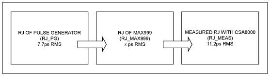
Figure 2. This flowchart illustrates the sequence from which we are able to extrapolate the jitter of the MAX999. Knowing that the HP8082A pulse generator contributes 7.7ps RMS, and that 11.2ps RMS is measured at the CSA8000, we are able to use Equation 1 to extrapolate the MAX999's jitter.
From this equation, we are able to determine that the MAX999 has a random jitter of 8.1ps RMS.
Basic Assumptions and Sources of Error in the Jitter Measurement
The 8.1ps RMS value is an estimate of the MAX999's real jitter. As has already been pointed out, this estimate is based on some basic assumptions and is affected by the following sources of error:
- The 1ps RMS jitter of the CSA8000 affects the measurement and causes an uncertainty of about 9%.
- It has been assumed that the jitter of the MAX999 is caused only by random jitter related to the thermal noise of the comparator itself and the surrounding resistors. The deterministic jitter is assumed to be very negligible.
- The noise contribution of the two 100Ω resistors that create the 2.5V at the MAX999's negative input is negligible (0.9nV/√Hz) and limited in bandwidth by the 7kHz low-pass filter formed with the capacitors in parallel.
- The noise contribution of the 200Ω output series resistor (1.8nV/√Hz) may create another source of error because it is not limited in bandwidth. However, as shown in the next section, this contribution is negligible compared to the MAX999's contribution.
- The jitter of the HP8082A pulse generator and the MAX999 have been considered uncorrelated.
Jitter-Noise Relationship
This random jitter is caused by the thermal (white) noise of the MAX999 and resistors. Refer to Application Note 3631: Random Noise Contribution to Timing Jitter—Theory and Practice for a background explanation of how random jitter and input-referred white noise are related in an amplifier. Near its switching point, a comparator behaves similar to an amplifier; specifically, the gain of the comparator stages makes the output switch as a consequence of an imbalance at the two inputs. Application Note 3631 shows that the RMS values of random jitter and white noise are related by the slew rate of the input (sinusoidal) signal, which is described by Equation 2:
JitterRMS = VnRMS/SR
The HP8082A pulse generator is so limited in bandwidth that the pulses at 80MHz appear as sine waves. For a sine wave, the slew rate in proximity of the zero crossing is given by Equation 3:
SR = A × 2 × π × ƒ
where A is the amplitude of the sine wave (in this case, 0.5V or 1VP-P) and ƒ is the frequency (in this case, 80MHz). This gives a slew rate of about 250V/µs = 250µV/ps. Therefore, the input-referred voltage noise over the 80MHz bandwidth can be calculated using Equation 4:
VnRMS = 250µV/ps × 8.1ps = 2025µVRMS
The contribution of the 200Ω series resistor over the same bandwidth is 14.3µVRMS, which can be considered negligible. Therefore, the main contribution to the overall random noise is from the MAX999 itself.
Conclusion
In some applications where a comparator is used to square off high-speed sinusoidal signals in order to generate a clock signal, it is important to know the output jitter specification of the comparator. This application note has shown how to extrapolate the output jitter measurement of the MAX999 even in the presence of a nonideal source generator. The limitation of this measurement and its sources of error have been discussed. Finally, the output jitter has been correlated with the input-referred voltage noise.
1 For a more detailed discussion of jitter, refer to Application Note 1916: An Introduction to Jitter in Communications Systems.