Digital Output Drivers: Understanding Key Features and Challenges
要約
This application note explains key features of the MAX14912/MAX14913 octal digital output driver and how they can be utilized in Industrial and Building Automation Applications.
Introduction
Digital output drivers are widely used in industrial applications for process control (PLC systems) and building automation. They also can be used anywhere a 24V DC system is used for control such as for motor control, robotics, and machinery automation.
At first look, the digital output driver is a simple device with only two output states: ON or OFF. On closer inspection, designers successfully replaced mechanical switches and relays providing engineers with many benefits like robust operation, low-power consumption, simplicity, smaller size, flexibility, and programmability to build automated, fault-tolerant control systems.
Maxim’s digital output drivers features up to 200kHz switching rates, fast and safe inductive load demagnetization, open load, low- and under-voltage detection, overcurrent and over-temperature protection, watchdog timer, and SPI error detection. They can withstand up to 60V power spikes, are immune to ±1kV surge pulses and up to 12kV ESD impact, and operate across a wide operating temperature range from -40°C to +125°C.
In this application note, we discuss how to effectively utilize different features of the MAX14912/MAX14913 output drivers. To do this, we look at the decisions a system designer must take and look at the trade-offs and benefits the MAX14912/MAX14913 provides.
Determine System Operating Conditions
High Side (HS) or Push Pull (PP)?
Usually the push-pull operation is used for high-speed communication, where the signal waveform should have sharp edges. The drawback of this mode is the output is always active, either high or low, and cannot be tristate or have high impedance, unless the Global EN pin is used.
High-side operation, instead, allows the engineer to put the output into a high-impedance state, but the signal waveform is largely dependent on the load impedance. The outputs can also be connected in parallel allowing larger loads up to 9.6A in high-side mode.
Therefore, selecting the operating mode depends on the particular application.
Power Supply Requirement
The MAX14912/MAX14913 supports a wide range of power supplies from 12V to 36V, that allows them to be used in a wide range of applications, even in systems with power supply requirements that are less regulated and more tolerant. This guarantees robustness and flexibility of the system design.
An integrated 5V DC-DC converter eliminates additional power rails, minimizes the number of external components, and increases the system efficiency. Other devices in the system can be powered from this 5V DC source, which can provide more than 100mA of current to the external circuits.
System Integration
The digital output drivers are the interface between low-voltage MCUs/FPGAs and relatively high-voltage (12V to 36V) peripheral devices, such as actuators, motors, lamps, relays, LEDs, etc. They provide high immunity to the voltage and current spikes, inductive or capacitive loads, and magnetic interference and static discharges.
In addition, the MAX14912/MAX14913 provide extensive diagnostic capabilities including thermal shutdown, open-wire detection, low-supply and undervoltage detection, and overvoltage and overcurrent protection. The 4 × 4 LED-driver crossbar matrix allows indication per channel for output status and fault conditions.
Digital Interface
There are two interfaces supported by the MAX14912 and MAX14913; parallel and serial. The system designer has flexibility to use either parallel or serial interface to control the operation, or to use both interfaces. To understand the interfaces, we first review a few of the global configuration pins.
Global Configuration Pins
EN – driving this pin high enables normal operation of the device; driving this pin low disables any output operation, i.e. makes all outputs high-impedance.
SRIAL – driving this pin high enables serial (SPI) operation; driving this pin low enables parallel operation.
PUSHPUL – driving this pin high enables push-pull mode of operation; driving this pin low or left unconnected results in all output pins operating in high-side mode.
FLTR – when this pin is set high, glitch filtering on all parallel logic inputs and CS pin are enabled.
Parallel Interface
The parallel interface is a simple pin-based interface to control the driver output. The device is controlled through the parallel interface if the SRIAL pin is tied to ground (SRIAL = low). The state of the OUT_ pin is controlled by the corresponding IN_ pin and state of the global configuration pins: PUSHPL, FLTR and EN. A minimum of nine GPIO pins are required to control the MAX14912/MAX14913 in parallel mode: controlling eight input pins IN_ and the PUSHPL pin. The FLTR and EN pin can be held high all the time. Pin settings are summarized in Table 1.
| PUSHPL | Driver Mode | IN_ | OUT_ state |
|---|---|---|---|
| 0 | High-side | 0 | High-side driver off/High impedance |
| 0 | High-side | 1 | High-side driver on/Output high |
| 1 | Push-pull | 0 | Output low |
| 1 | Push-pull | 1 | Output high |
Note: the MAX14913 does not allow serial configuration in parallel mode whereas the MAX14912 can be configured through the serial interface even if SRIAL is low. All registers, except register 0, are accessible in this mode (refer to Serial Interface section below).
Configuration through the serial interface has a higher priority over the PUSHPL pin settings. Logic level 0 (low) or 1 (high) depends on the VL input, which is valid from 1.6V to 5.5V. The drawback of parallel mode is the lack of diagnostic information.
Serial Interface
The serial, SPI interface, is enabled when the SRIAL pin is driven to VL level (SRIAL = high). In serial mode, all output pins are controlled by internal register settings and input pins. The registers can be accessed through the serial interface pins: CS, CLK, SDI and SDO. Refer to the serial interface section in the MAX14912/MAX14913 data sheet for details.
Some features, such as cyclic-redundancy check (CRC), watchdog, and filtering are controlled only by input logic on CRC/IN3, WDEN/IN5 and FLTR pins, while open load detection and output configuration are controlled by either input logic on OL/IN1 and PUSHPL pins, or through registers settings.
In addition, settings of CMND/IN2, CNFG/IN7 and S16/IN8 are summarized in Table 2.
| PIN | RESULT | |||||||
|---|---|---|---|---|---|---|---|---|
| SPI MODE | SRIAL | CMND/IN2 | CNFG/IN7 | S16/IN8 | BITS | SDI | SDO | NOTES |
 |
1 | 0 | 1 | 0 | 8 | Per-channel fault | OUT set by SPI. FAULTis the real-time status of the fault (driver shutdown or open-load | |
| 1 | 16 | Per-channel fault and level | ||||||
| 1 | 0 | 1 | 0 | 8 | Per-channel fault | OUT level does not change | ||
| 1 | 16 | Per-channel fault and level | ||||||
 |
1 | 1 | X | X | 16 | Previous command output | OUT level may or may not change depending on command | |
| 0 | X | X | X | 16 | Previous command output | OUT set by INx pins. MAX14912 allows SPI configuration. MAX14913 does not allow SPI configuration. | ||
Direct Mode
In direct SPI mode, no command byte is needed. The high byte controls the output levels and low byte the output configuration in 16-bit mode. Only Reg. 0 is accessible when the CNFG/IN7 and S16/IN8 are set low. Only Reg. 1 and Reg. 2 are accessible when CNFG/IN7 and S16/IN8 are set high.
Fault (F) and output level (L) diagnostic is available on the SDO pin during direct-mode write (refer to Figure 1 and Table 3).
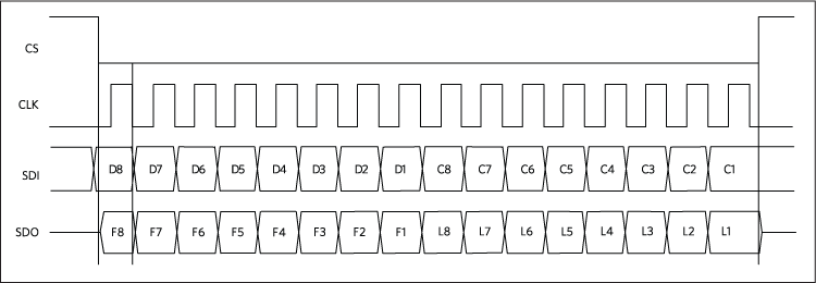
Figure 1. SPI cycle in 16-bit direct SPI mode.
| BIT | BIT VALUE | CNFG/IN7 | DEFINITION |
| D_ | 0 | Low |
In high-side mode: HS off, LS off In push-pull mode: HS off, LS on |
| 1 | Low | Low HS on, LS off | |
| C_ | 0 | Low | High-side mode |
| 1 | Low | Push-pull mode | |
| D_C- | 00 | High | High-side mode; open load detection defined by OL/IN1 pin |
| 01 | High | High-side mode with open-load detection | |
| 10 | High | Push-pull mode | |
| 11 | High | Not used | |
| 00 | Low | High-side mode: HS off, LS off | |
| 10 | Low | High-side mode: HS on, LS off | |
| 01 | Low | Push-pull mode: HS off, LS on | |
| 11 | Low | Push-pull mode: HS on, LS off | |
| F_ | 0 | X | No fault |
| 1 | X | Fault status (thermal protection or open-load) | |
| L_ | 0 | 0 | Output level < 7V |
| 1 | 0 | Output level > 7V | |
| 0 | 1 | Slow mode disabled | |
| 1 | 1 | Slow mode disabled |
In summary,
- when S16/IN8 = low and CNFG/IN7 = low, one byte of serial data controls the OUT_ state; when S16/IN8 = low and CNFG/IN7 = high, one byte of serial data controls the output mode: high-side or push-pull.
- when S16/IN8 = high and CNFG/IN7 = low, two bytes of serial data control both the OUT_ state and output mode configuration: high-side or push-pull.
- when S16/IN8 = high and CNFG/IN7 = high, the first byte sets output configuration (high-side/push-pull) and the second byte enables/disables open-load detection.
It is recommended to set up configuration registers first and then update the output level.
Note: the returned F_ (fault) and L_ (level) info is for the previous written command. Write twice in order to get real-time fault and level diagnostic. When the driver is in high-side mode with open-load detection enabled, the OUT_ pin with no load is pulled high to VDD level by 75µA current. In this case FAULT condition is determined.
Command Mode
In command mode all features and enhanced diagnostic are available through the SPI interface. To set a command mode the CNMD/IN2 pin must be set high. The inputs of the S16/IN8 and CNFG/IN7 pins are ignored. The command contains the command byte followed by the data byte. There are total of six command types available (see Table 4 for command description and Table 5 for Registers map). For more information, refer to the data sheet.
| COMMAND # | FUNCTION | DI | DO | COMMENTS | |
|---|---|---|---|---|---|
| COMMAND | DATA | VALID ON NEXT CYCLE | |||
| 0 | Set OUT state (reg. 0) | Z0000000 | DDDDDDDD | FFFFFFFF.LLLLLLLL | D = 0: HS off; LS on (in PP)
D = 1: HS on; LS off L: output level or Slow mode (CNFG = 1) F: fault (real-time) Z = 1: clear fault registers |
| 1 | Set HS/PP nide (reg. 1) | Z0000001 | DDDDDDDD | FFFFFFFF.LLLLLLLL |
D = 0: HS mode D = 1: PP mode |
| 2 | Set OL detection (reg. 2) | Z0000010 | DDDDDDDD | FFFFFFFF.LLLLLLLL |
D = 0: OL detection off D = 1: OL detection on (HS mode) |
| 3 | Set Configuration (reg. 3 | Z0000011 | 000SJJAV | FFFFFFFF.LLLLLLLL | AB: watchdog 00 = 0.90s 01 = 0.45s 10 = 0.15s J = 1: channels are coupled (PP disabled) S = 1: FAULT not asserted when short-circuit is detected |
| 4 | Read Register | Z0100000 | 00000NNN | AAAAAAAA.QQQQQQQQ | NNN = 0,1,2,3: Q = reg. value, A = 0 NNN = 4,5,6: Q = reg. value, A = real-time fault status NNN = 7: Q = 0, A = real-time |
| 5 | Read Real-Time Status | Z0110000 | 00000000 | FFFFFFFF.LLLLLLLL | F-L status read-out (real-time). No data is written. |
| Note: All fault registers are cleared only by setting Z = 1 with any command cycle. | |||||
| REG | R/W | PURPOSE | 7 | 6 | 5 | 4 | 3 | 2 | 1 | 0 |
|---|---|---|---|---|---|---|---|---|---|---|
| 0 | R/W | Driver Settings | IN8 | IN7 | IN6 | IN5 | IN4 | IN3 | IN2 | IN1 |
| 1 | R/W | Push-Pull/High-Side Configuration | PP8 | PP7 | PP6 | PP5 | PP4 | PP3 | PP2 | PP1 |
| 2 | R/W | R/W Open Load Detect Enable | OL_EN8 | OL_EN7 | OL_EN6 | OL_EN5 | OL_EN4 | OL_EN3 | OL_EN2 | OL_EN1 |
| 3 | R/W | Watchdog Config. And Channel Paralleling | X | X | X | Short-circuit Pulse OFF | joinUP | joinDW | WD1 | WD0 |
| 4 | R | Per-Channel Open-Load Condition | OL8 | OL7 | OL6 | OL5 | OL4 | OL3 | OL2 | OL1 |
| 5 | R | Per-Channel Thermal Shutdown | THSD8 | THSD7 | THSD6 | THSD5 | THSD4 | THSD3 | THSD2 | THSD1 |
| 6 | R | Global Faults | WDfault | CRCfault | DCDC Current Limit |
8CLKmult Error | THSDglob | 5V UVLO | VDD UVLO | VDD WARN |
| 7 | R | OUT Overvoltage Detection or Slow mode | OV8 | OV7 | OV6 | OV5 | OV4 | OV3 | OV2 | OV1 |
Communication Error (CRC Detection)
A cyclic-redundancy check (CRC) is an error detecting feature that allows increased communication reliability and avoids accidentally executing unintended commands. Initially, the SPI protocol does not have any error detection capability and serial data can be corrupted in harsh industrial environments. When the CRC detection is enabled (SRIAL= high and CRC/IN3 = high), all commands from the SPI master must be followed by an additional byte with the 7-bit CRC code, as shown in Figure 2.

Figure 2. SDI check byte expected from microcontroller.
The 7-bit CRC code, also known as CRC frame-check sequence (FCS), is calculated based on the generator polynomial (x7 + x5 + x4 + x2 + x + 1). The same polynomial also used in MAX14900E. For more information and examples of C-code implementation of the CRC calculation, refer to application note 6002, "CRC Programming for the MAX14900E Octal, High-Speed Industrial Switch."
When either the MAX14912 or MAX14913 is installed, the device checks the received data for bit corruption and execute the command if no error is detected. If the CRC code received from the microcontroller does not match with the calculated CRC, the command is ignored and CRC error bit 6 is set in Register 6. The CRC error is reported to the host microcontroller on the next SPI frame.
The CRC calculator is built into the MAX14912EVKIT software. If the CRC/IN3 pin is driven high, the CRC byte automatically calculates and adds to the SPI command frame. It can be seen in the Status Log window if the Show Status Log option is selected from the Option menu.
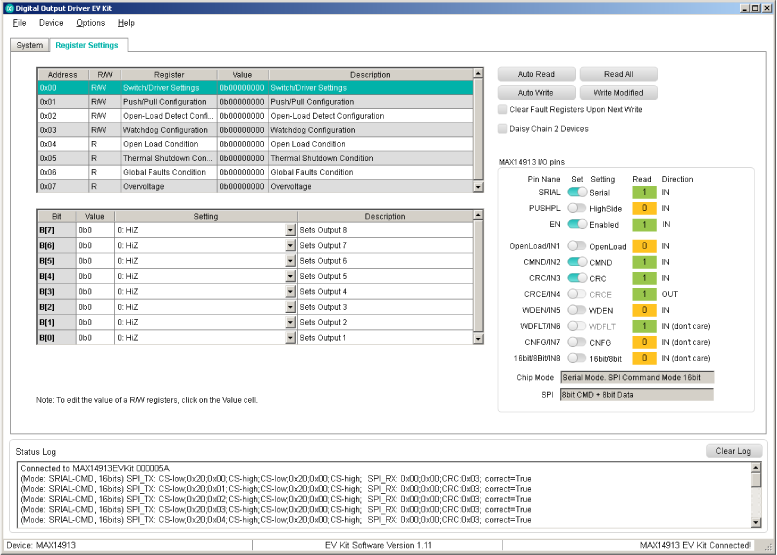
Figure 3. CRC calculation in the digital output driver GUI.
CRC code can be manually calculated in the CRC calculator pop-up window. Go to the Help menu and click on the CRC calculator to bring it up. Type in the value of Byte 1 and Byte 2 and click the Calculate CRC button as shown in Figure 4.
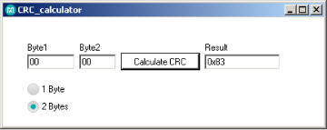
Figure 4. CRC calculator pop-up window.
Daisy Chaining of Multiple ICs
The MAX14912 and MAX14913 allows daisy chaining of multiple devices and control/monitor all devices on the same SPI bus simultaneously by a single command pattern. All devices use the common CLK and CS signals; the SDI pin of the first device in a chain is connected to the master’s MOSI pin and the SDO of the last device is connected to the master’s MISO pin. The data-out (SDO) of the first device connects to the data-in (SDI) of the second device, as shown in Figure 5. Other devices can be daisy chained in a similar manner.
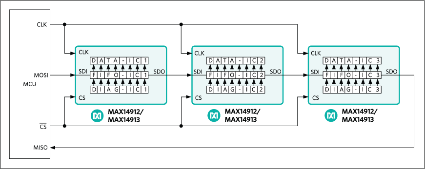
Figure 5. Daisy-Chain Connection.
The MAX14912/MAX14913EVKIT allows daisy chaining of two EVKITs, but the same command structure applies to three or more devices.
For example, command frame for two daisy chained devices in 16-bit Command Mode.

The EVKITs should be stacked so that the J24 header of the following device, EVKIT #2, is connected to J23 of EVKIT #1, as shown in Figure 6. The USB cable or external master should be connected to EVKIT #1. In addition, the J26 jumper of EVKIT #1 must be in position 2 to 3, but the J26 jumper of EVKIT #2 should be in position 1 to 2. Jumpers on the J9, J5, J4, J22, J10, J6, J12, JMP1, J11, JMP2, J8 and J3 of EVKIT #2 have to be manually set to the same position as in the GUI. For more information, refer to the MAX14912/MAX14913 data sheet and schematic.
Figure 6. Daisy-chaining MAX14912EVKITs.
The daisy chain box should be selected as shown in Figure 7.
Figure 7. Daisy-chain operation.
The ability to daisy chain is not limited to extending the number of output channels, but also to allow to build more sophisticated systems in combination with a digital output driver and a digital input receiver, such as octal digital input translator/serializer family, the MAX31910/MAX31913.
Driving Inductive Loads
The MAX14912 and MAX14913 feature safe demagnetization (SafeDemag) of an inductive load, which prevents damaging the chip by the kickback voltage created when turning off an inductive load in high-side mode. If you need to drive a large inductance, e.g. actuator, relay or motor, a large amount of energy is stored in the inductive load when current flows from the chip through the load to ground. When the current is terminated by the high-side switch turning off, that energy is transformed into a negative spike on the OUT_ pins. The spike is clamped by an internal Zener diode to the level of (VDD - 56V). For example, if VDD = 24V, then the OUT_ pin is clamped to -32V relative to ground. In this case, the energy stored in the inductive load dissipates faster since the energy is proportional to |V x I|. However, dissipation of a larger energy requires more time. During that time the chip’s temperature can reach the safety threshold. To prevent dangerous thermal runaway, the low-side switch is activated allowing less energy dissipation until the internal temperature meets the safe region.
Conclusion
Maxim’s family of highly integrated digital output drivers provides a tremendous amount of robustness, flexibility and features to the system designer. They are the key elements to build highly integrated and efficient control systems for any industrial automation and communication applications.