Design Porting Considerations for the MAX2870
要約
This application note compares the MAX2870 ultra-wideband synthesizer/voltage controller oscillator (VCO) to the Analog Devices ADF4350 synthesizer. Registers and loop filter design are discussed in detail.
The MAX2870 ultra-wideband phase-locked loop (PLL) and voltage control oscillator (VCO) can operate in both integer-N and fractional-N modes, similar to the Analog Devices ADF4350 wideband synthesizer. This application note compares the MAX2870 and ADF4350 registers and loop filter design in detail. Users who already familiar with ADF4350 can use this application note as a quick design reference.
Register Table Comparison
Register 0
| Bit Position | MAX2870 | ADF4350 | Difference | ||
| Bit ID | Name/Description | Bit ID | Name/Description | ||
| 31 | INT | Int-N or frac-N mode control | — | Reserved | The MAX2870 provides an additional method to switch between int and frac modes (Note 1). |
| 30–15 | N[15:0] | Integer division value | N16– N1 | Integer value | Both are 16-bit resolution, but the MAX2870 offers a wider usable range. See the MAX2870 data sheet for details. |
| 14–3 | FRAC[11:0] | Fractional division value | F12– F1 | Fractional value | N/A |
| 2–0 | ADDR[2:0] | Register address | C3– C1 | Register address | N/A |
Register 1
| Bit Position | MAX2870 | ADF4350 | Difference | ||
| Bit ID | Name/Description | Bit ID | Name/Description | ||
| 31 | CPOC | CP output clamp: set to 1 for int mode; set to 0 for frac mode | — | Reserved | The MAX2870 provides programmability on the CP output clamp to achieve better noise performance in int-N mode. |
| 30–29 | CPL[1:0] | CP linearity: set to 00 for int mode; set to 01 for frac mode | — | Reserved | The MAX2870 provides programmability for CP linearity to achieve better spurious performance in frac-N mode. |
| 28 | CPT[1] | Charge pump test mode: 00 for normal operation; 10 for CP in source mode; 11 for CP in sink mode | — | Reserved | On the ADF4350, users set bit 27 to program the prescaler value. On the MAX2870, the prescaler is automatically set. Users must set only CPT[1:0] to 00 for normal operation. |
| 27 | CPT[0] | PR1 |
Prescaler | ||
| 26–15 | P[11:0] | Phase value | P12– P1 | Phase value | N/A |
| 14–3 | M[11:0] | Modulus value | M12– M1 | Interpolator modulus | N/A |
| 2–0 | ADDR[2:0] | Register address | C3– C1 | Register address | N/A |
Register 2
| Bit Position | MAX2870 | ADF4350 | Difference | ||
| Bit ID | Name/Description | Bit ID | Name/Description | ||
| 31 | LDS | Lock detect speed | — | Reserved | The MAX2870 provides 4ns lock detect precision when PFD frequency is greater than 32MHz (Note 2). |
| 30–29 | SDN[1:0] | Frac-N noise mode 00 = low-noise mode 01 = reserved 10 = low-spur mode 1 11 = low-spur mode 2 |
L2– L1 | Noise mode 00 = low-noise mode 01 = reserved 10 = reserved 11 = low-spur mode |
The MAX2870 provides two modes of dithering for spur mitigation. Users should choose the one that works best in their system. |
| 28–26 | MUX[2:0] | MUX_OUT configuration |
M3– M1 | MUXOUT | The MAX2870 has the same mux output, plus an extra serial output to be read out of Register 6 (Note 3). |
| 25 | DBR | Reference doubler mode | RD2 |
Reference doubler | N/A |
| 24 | RDIV2 | Reference Div2 mode | RD1 | Reference divideby2 | N/A |
| 23–14 | R[9:0] | Reference divider mode | R10– R1 | 10-bit R counter | N/A |
| 13 | REG4DB | Double buffer | D1 | Double buffer | N/A |
| 12–9 | CP[3:0] | Charge-pump current | CP4– CP1 | Charge pump current setting | N/A |
| 8 | LDF | Lock-detect function | U6 | LDF | N/A |
| 7 | LDP | Lock-detect precision | U5 | LDP | N/A |
| 6 | PDP | Phase detector polarity | U4 | PD POLARITY | N/A |
| 5 | SHDN | Power-down mode | U3 | Power down | N/A |
| 4 | TRI | Charge-pump three-state mode | U2 | Cp three state | N/A |
| 3 | RST | Counter reset | U1 | Counter reset | N/A |
| 2–0 | ADDR[2:0] | Register address | C3– C1 | Register address | N/A |
Register 3
| Bit Position | MAX2870 | ADF4350 | Difference | ||
| Bit ID | Name/Description | Bit ID | Name/Description | ||
| 31–26 | VCO[5:0] | Manual VCO selection and VCO subband when VAS is disabled | — | Reserved | The MAX2870 allows the user to disable VCO autoselection (VAS) machine and manually select VCO subband. Use this function with a VCO lookup table method to achieve faster PLL lock time. |
| 25 | VAS_SHDN | VAS SHDN: 0 = VAS enabled; 1 = VAS disabled |
— | Reserved | |
| 24 | RETUNE | Sets VAS response to temperature drift | — | Reserved | |
| 23–19 | >— | Reserved | — | Reserved | N/A |
| 18 | — | Reserved | F1 | CSR | Yes |
| 17 | — | Reserved | — | Reserved | N/A |
| 16–15 | CDM[1:0] | Clock divider mode: 10 = phase mode |
C2– C1 | Clock div mode: 10 = resync mode |
The MAX2870 only provides a phase change from the current phase, where the ADF4350 allows a phase relative to a sync pulse. |
| 14–3 | CDIV[11:0] | Clock divider value | D12– D1 | 12-bit clock divider value | These bits define the low-frequency clock ratio on both parts; depending on operation mode, they have different meanings (Note 4). |
| 2–0 | ADDR[2:0] | Register address | C3– C1 | Register address | N/A |
Register 4
| Bit Position | MAX2870 | ADF4350 | Difference | ||
| Bit ID | Name/Description | Bit ID | Name/Description | ||
| 31–26 | — | Reserved | — | Reserved | Set to 011000 on the MAX2870. |
| 25–24 | BS_MSBs[1:0] | Band-select MSBs | — | Reserved | Because the MAX2870 allows higher PDF frequency, these additional bits increase the band-select divider range from 8 to 10 bits. |
| 23 | FB | VCO feedback mode | D13 | Feedback select | N/A |
| 22–20 | DIVA[2:0] | RFOUT_ output divider mode | D12– D10 | RF divider select | The MAX2870 provides more RFOUT divider ratio options (Note 5). |
| 19–12 | BS[7:0] | Sets band-select clock-divider value. MSBs are located in bits <25:24> | BS8– BS1 | 8-bit BAND select clock divider value | Same for the 8-bit band-select divider. The MAX2870 offers two more MSBs (see BS_MSBs[1:0]). |
| 11 | — | Reserved | D9 | VCO power down | Yes |
| 10 | — | Reserved | D8 | Mute till lock detect | Yes |
| 9 | BDIV | RFOUTB output path select | D7 | AUX out select | N/A |
| 8 | RFB_EN | RFOUTB output mode | D6 | AUX out enable | N/A |
| 7–6 | BPWR[1:0] | RFOUTB output power | D5– D4 | AUX out power | N/A |
| 5 | RFA_EN | RFOUTA output mode | D3 | RF out enable | N/A |
| 4 | APWR[1:0] | RFOUTA output power | D2– D1 | Output power | N/A |
| 2–0 | ADDR[2:0] | Register address | C1 | Register address | N/A |
Register 5
| Bit Position | MAX2870 | ADF4350 | Difference | ||
| Bit ID | Name/Description | Bit ID | Name/Description | ||
| 31–25 | — | Reserved | — | Reserved | N/A |
| 24 | F01 | F01 | — | — | The MAX2870 provides an additional method to control int/frac mode (Note 1). |
| 23–22 | LD[1:0] | Lock-detect pin function | D15– D14 | LD PIN mode | N/A |
| 21–19 | — | Reserved | — | Reserved | N/A |
| 18 | MUX[3] | MUX MSB | — | Reserved | The MAX2870 provides additional serial data output on MUX pin (Note 3). |
| 17 | — | Reserved | — | Reserved | N/A |
| 16–3 | — | Reserved | — | Reserved | N/A |
| 16–3 | — | Reserved | — | Reserved | N/A |
| 2–0 | ADDR[2:0] | Register address | C3– C1 | Register address | N/A |
Loop Filter
The MAX2870's KVCO (typical 100MHz/V) is different than the ADI4350's (typical 33MHz/V). To keep PLL parameters (e.g., CP current, N divider, Fcomp, loop BW, and phase margin) unchanged, the loop filter components must be recalculated (Figure 1). Using ADI4350's loop filter on the MAX2870 without careful evaluation could result in performance degradation or even unstable PLL.
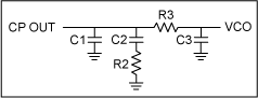
Figure 1. Loop filter component labels.
The following example shows that to maintain the PLL's parameters, a different loop filter needs to be installed, depending on whether the MAX2870 or ADI4350 is being used.
| PLL Condition and Loop Filter | MAX2870 | ADF4350 | Notes |
| KVCO (MHz/V) | 100 | 33 | Different KVCO |
| ICP (mA) | 2.5 | 2.5 | Same |
| Fcomp (MHz) | 10 | 10 | Same |
| N | 400 | 400 | Same |
| Loop BW (kHz) | 20.2 | 17.6 | Similar loop BW |
| Phase margin (deg) | 39 | 37.5 | Similar phase margin |
| C1 (nF) | 10 | 1.5 | Different loop filter |
| C2 (nF) | 68 | 22 | Different loop filter |
| R2 (Ω) | 220 | 430 | Different loop filter |
| C3 (nF) | 1.2 | 0.68 | Different loop filter |
| R3 (Ω) | 1000 | 820 | Different loop filter |
Notes
Note 1: The MAX2870 has two methods for switching between int/frac modes. In Method 2, this is independent of the FRAC[11:0] bit setting.
| Int/Frac Mode Switching | MAX2870 | ADF4350 | Notes | |||
| F01 | INT | FRAC11– FRAC00 | FRAC11– FRAC00 | |||
| Method 1 | Integer mode | 1 | X | All 0s | All 0s | N/A |
| Frac mode | 1 | X | Not all 0s | Not all 0s | N/A | |
| Method 2 | Integer mode | 0 | 1 | X | N/A | The MAX2870 provides an additional method. |
| Frac mode | 0 | 0 | X | N/A | The MAX2870 provides an additional method. | |
Note 2: The MAX2870 allows users to set a PDF frequency of up to 105MHz in int mode, and up to 50MHz in frac mode. The table below summarizes the LD pin settings under different PDF frequencies.
| LD Pin Function | MAX2870 | ADF4350 | Notes | |||||
| LD[1:0] | LDS | LDP | LDF | D15–D14 | LDP | LDF | ||
| Low | 00 | X | X | X | 00 | X | X | Same as ADF4350 |
| Digital LD | 01 | 0 | 0 | 0 | 01 | 0 | 0 | Same as ADF4350, for PDF frequency < 32MHz, frac-N mode, 10ns precision |
| 0 | 0 | 1 | 0 | 1 | Same as ADF4350, for PDF frequency < 32MHz, integer mode, 10ns precision | |||
| 0 | 1 | 0 | 1 | 0 | Same as ADF4350, for PDF frequency < 32MHz, frac-N mode, 6ns precision | |||
| 0 | 1 | 1 | 1 | 1 | Same as ADF4350, for PDF frequency < 32MHz, integer mode, 6ns precision | |||
| 1 | X | 0 | — | — | The MAX2870 digital LD function for PDF frequency > 32MHz, frac-N mode, 4ns precision | |||
| 1 | X | 1 | — | — | The MAX2870 digital LD function for PDF frequency > 32MHz, int mode, 4ns precision | |||
| Analog LD | 10 | X | X | X | 10 | X | X | Same as ADF4350 |
| High | 11 | X | X | X | 11 | X | X | Same as ADF4350 |
Note 3: The table below summarizes the MUX pin setting of the MAX2870 and ADF4350.
| MUX Pin Function | MAX2870 | ADF4350 | Notes | ||
| MUX[3] REG5[18] | MUX[2:0] REG2[28:26] | REG5[18] | M3–M1 REG2[28:26] | ||
| Regular MUX pin function | 0 | 000–111 | Reserved | 000–111 | N/A |
| Serial data output | 1 | 100 | — | — | The MAX2870 configures the MUX_OUT pin as serial data output to read REG 06 (IC status bits). The ADF4350 does not have this function. |
Note 4: Below is a comparison of the CDIV bits function under different modes.
| Operation Mode | MAX2870 | ADF4350 |
| CDIV[11:0], Reg3[14:3] | D12-D1, Reg3[14:3] | |
| Fast lock mode | CDIV defines the fast lock timeout | Defines the fast lock timeout |
| Phase adjust mode | Adjusts the VCO phase relative to the current phase, so no resync period is necessary | D12-D1 define the phase resync period. |
Note 5: The MAX2870 provides more output divider ratio selection, allowing more design flexibility.
| Output-Divider Ratio | MAX2870 | ADF4350 |
| DIVA[2:0], Reg4[22:20] | D12–D10, Reg4[22:20] | |
| 1 | 000 | 000 |
| 2 | 001 | 001 |
| 4 | 010 | 010 |
| 8 | 011 | 011 |
| 16 | 100 | 100 |
| 32 | 101 | Not available |
| 64 | 110 | Not available |
| 128 | 111 | Not available |