AN-920: Gain, LO, and Phase Compensation in a Single Sideband Transmitter Using the AD9788 TxDAC and ADL5372 Quadrature Modulator
Introduction
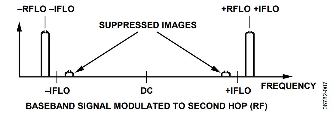
In a traditional radio transmit (Tx) architecture, a baseband signal (voice or data), is modulated to an intermediate frequency (IF) and then modulated again to the transmit radio frequency (RF). Traditionally, inexpensive upconverting modulators only provide good performance over roughly one decade of frequency conversion, so it is often necessary to execute the complete upconversion in two or more frequency hops as shown in Figure 1. Note that with two hops, a second spectral image is produced that has no value for the transmitter. In fact, to meet spectral mask specifications (so as not to interfere with other transmitters and receivers), this image must often be filtered, a task which is not always an easy or inexpensive thing to do at the RF frequency. Also note in Figure 1 that using the AD9788, the redundant images and LO feedthrough can be suppressed to the noise floor.
A single sideband transmitter, on the other hand, uses complex mathematical techniques to suppress the unwanted negative frequency image. In addition, by using these mathematical techniques rather than filtering, two channels of data can be transmitted within the same bandwidth, thus doubling spectral efficiency. This is done by placing one channel of data on a cosinusoidal carrier (the I data) and the other channel of data on a sinusoidal carrier (the Q data), with both carriers set to the same frequency. Modern receivers have the ability to separate signals on these quadrature carriers, and to separate the I data from the Q data.
This application note describes how to use the AD9788 TxDAC® as a key component in a single sideband transmitter where a high dynamic range IF signal is required at the DAC output. The complex numerically controlled oscillator (NCO) in the AD9788 enables this architecture, and the programmable gain and offset matching, as well as phase compensation in the AD9788 allow the user to calibrate out unwanted artifacts of the complex modulation. This optimizes performance and lessens the need for additional filtering and/or more rigorous frequency planning to reduce the effects of these artifacts.
The AD9788 offers excellent dynamic range and can generate complex IF frequencies up to 400 MHz. Using the NCO alone typically provides image and LO suppression of −40 dBc over the operating temperature range of the components. Using the calibration techniques described in this application note can lower these components to −60 dBc or better. Note, however, that the performance becomes much more temperature sensitive, and algorithms must be used to sense and to compensate for these temperature shifts.


Single Sideband Modulation
The modulation shown in Figure 1 is often referred to as real modulation. A real signal, in mathematical terms, refers to a signal with identical positive and negative frequency components. The fact that the modulating signals IFLO and RFLO are both real (containing both positive and negative frequency components) means that when these LOs operate on any signal, an image signal is created for both the negative and positive frequency components of the LO.
The alternative to real modulation is a technique called single sideband transmission. With single sideband transmission, the redundant image is phase shifted by 180° and then added back to the original signal. This suppresses the redundant image, without resorting to filtering. Single sideband transmission has been in use for several decades, but it has always required additional expensive components. In addition, because the components used were strictly analog and tended to drift over temperature, the amount of image suppression was limited. Due to the limited image rejection in a purely analog system, some amount of filtering was often necessary to achieve the desired performance.
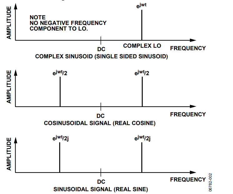
To realize a single sideband transmitter, the modulating LO must consist of only a positive or only a negative sinusoid, as opposed to the real modulator where the LO included both positive and negative frequency components. Engineering textbooks often refer to this single sided sinusoid as a complex sinusoid, and it is typically referred to mathematically as ejωt
In math textbooks, Euler’s equation is often cited, which states
ejωt = cosωt + j × sinωt
where j is equal to sqrt(−1)
The complex sinusoid, the real cosinusoid, and the real sinusoid are shown in Figure 2.

Realization of a Digital Single Sideband Modulator
To realize a single sideband modulation scheme in a circuit, start with a baseband signal referred to in this example as bb(t). Spectrally, this signal is the same as shown in Figure 1. If bb(t) drives the complex modulator, which is fed by a complex LO, as shown in Figure 2, the resulting output is
bb(t) × (cos(ωt) + j × sint(ωt))
This implies that the single sideband modulator has two outputs. One output represents the real component of the modulation (cosωt) and the other channel (sinωt) represents the imaginary component of the modulation. This is shown, schematically and spectrally, in Figure 3 .Taken as the real and imaginary components of the modulated baseband signal, the two signals represent single sideband modulation


It is often difficult to grasp, because it is somewhat abstract, that the complex signal is actually represented by two signals: one defined as real and the other defined as imaginary. Although the operation is somewhat contrived, the math holds up and the end result, as is evident after the second modulation hop, actually results in the suppression of the redundant image. It is also important to note that if a spectrum analyzer is used (which doesn’t show phase relationships) to view the real or imaginary modulator outputs at this point, no difference between this output and the real modulator output shown in Figure 1 is evident.
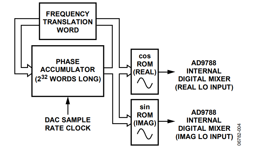
The Complex NCO in the AD9788
The solution for realizing the single sideband modulator, as described in this application note, is simple. The first requirement is for the generation of a LO, consisting of two components: one component is a cosinusoidal LO which represents the real LO, and the other component is a sinusoidal LO which represents the imaginary LO.
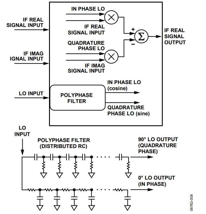
The AD9788 provides its own internal digital complex NCO. The length of the phase accumulator in the NCO is 232, which provides a very high frequency resolution. Because this is done digitally, with no elements of analog degradation, the 90° quadrature separation can be guaranteed over all process, voltage, and temperature shifts. The math in the digital engine does not vary with any of these parameters. Figure 4 shows a block diagram of the complex NCO used in the AD9788.
Programming the Complex NCO in the AD9788
The NCO in the AD9788 is controlled via the frequency translation word and phase control registers (Register 0xA and Register 0xB). For more information, refer to the AD9788 data sheet.

The AD9788 Quadrature Modulator
To understand the quadrature modulator, refer once more to Euler’s equation. As described in the Single Sideband Modulation section, this equation describes a complex carrier. Start by defining a baseband signal consisting of two components: real and imaginary. The baseband signal can then be defined as
Re(bb(t)) + j × Im(bb(t))
If this baseband signal is modulated onto the complex carrier (ejωt = cosωt +j × sinωt), the result of the modulation is two new signals, real and imaginary.
Real output =
Re(bb(t)) × cosωt − Im(bb(t)) × sinωt = Re(t)
Imaginary output =
Re(bb(t)) × sinωt + Im(bb(t)) × cosωt = Im(t)
Taking these two signals together as a complex channel gives the form
complexIF = Re(t) + j × Im(t)
Spectrally, the complex IF signal takes the form shown in Figure 3.
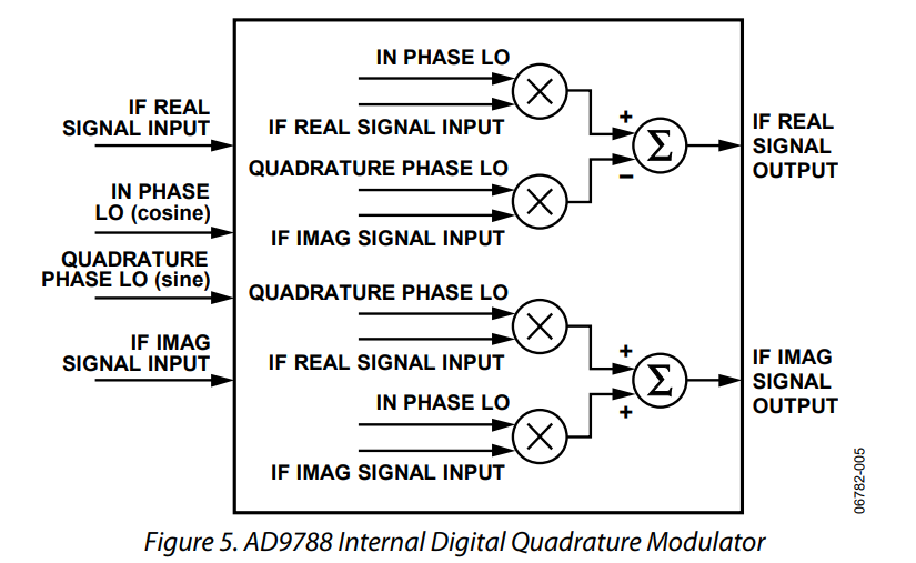
The Digital Quadrature Modulator
A block diagram of the digital quadrature modulator in the AD9788 is given in Figure 5. Taken together, the real and imaginary (usually referred to as the in phase and quadrature, or I and Q) outputs form a complex channel, which is something of a mathematical artifact. If a spectrum analyzer were used to view either channel, no amount of image rejection would be seen, as the spectrum analyzer does not give phase information.
It is also possible, by switching the sign on the lower input of each summing junction in Figure 5, to switch which image is passed and which image is rejected. If these signs are switched, the images at ±(RF − IF) are passed, and those at ±(RF + IF) are suppressed
As stated earlier, one of the benefits of the single sideband transmitter is that two channels of information are transmitted in the same bandwidth. This can be seen in the previous equations. However, the image rejection capability of this architecture is not realized in this one stage.
To completely enable a single sideband radio, a second complex modulation stage must be added. This second stage is very often done with an analog quadrature modulator, because RF signals in the multi GHz range required cannot currently be generated by low cost DACs. Analog quadrature modulators, unlike their digital counterparts, have gain matching, input offset matching and phase matching characteristics that do drift over temperature. The AD9788 has programmable features that allow the user to compensate for analog drift characteristics of the analog quadrature modulator.

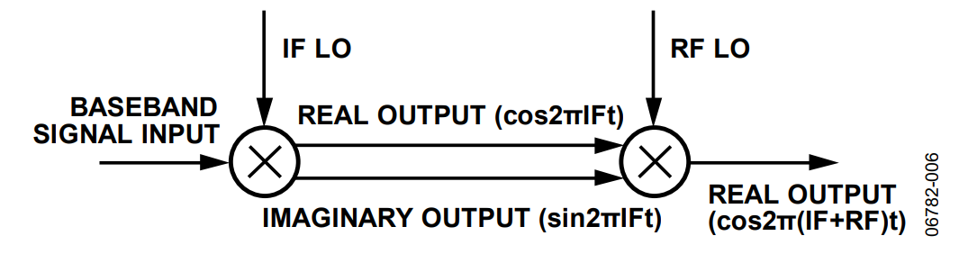
A simple block diagram of the two-step complex modulation process that results in the single sideband radio is shown in Figure 6. The actual spectrum is shown in Figure 7.
The image rejection is achieved at either the real or the imaginary outputs of the second complex modulation stage, so the use of both real and imaginary outputs is unnecessary. Therefore, this application note assumes that only the real output of the analog quadrature modulator is used.
Analog quadrature modulators typically only consist of the real side of the complete complex modulator. Of course, many other components must be used in and around this signal chain to achieve desired performance. These typically include passive Ls, Rs, and Cs, as well as filters of all types.
After the second quadrature modulator, there is typically more filtering, possibly a VGA for power control, and finally a power amplifier to drive the antenna.


The Analog Quadrature Modulator
Given the phase relationships between the real and imaginary components of the IF out of the DAC, using another quadrature modulator for the next stage causes the frequency components of the undesired frequency image to cancel each other out, as shown in Figure 7. Structurally, the analog quadrature modulator is similar to that of the digital quadrature modulator. The major differences are that the quadrature modulator has only a real output, and that many of the figures of merit of the quadrature modulator drift over temperature. For ease of use, a single LO input is designed in, and the phase splitting is achieved via an analog polyphase filter network. A block diagram of an analog quadrature modulator, and a simplified polyphase filter to achieve quadrature, are shown in Figure 8.
Some newer quadrature modulators, such as the ADL538x family from Analog Devices, Inc., actually require the externally applied LO to be 2× that of the required internal I LO and Q LO. With this type of modulator architecture, a polyphase filter is not required. With a 2× LO applied, perfect quadrature can be achieved on the internal I LO and Q LO over a wider bandwidth than can be achieved with any reasonably sized polyphase filter.

Common Circuit Implementations
In modern digital radio transmitters, a digital-to-analog converter (DAC) is used to convert the digital content of the signal to an analog format suitable for transmitting. Once this signal is in an analog format, an analog quadrature modulator is used to convert to RF. This signal chain often takes the form shown in Figure 9.

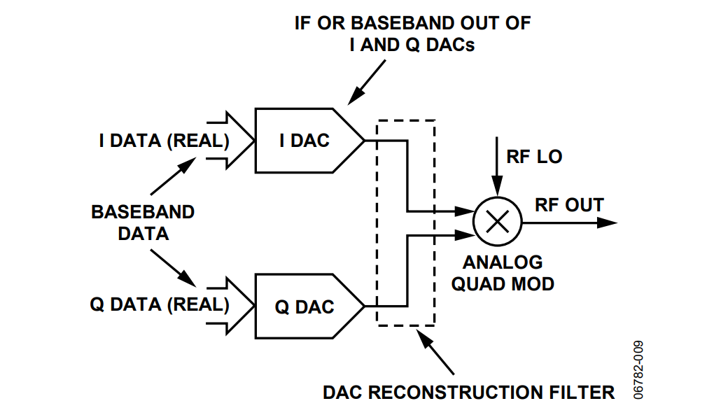
The digital content at the input to the DAC can take several forms. It can consist of real or complex baseband data, or it may already be modulated onto an IF. Using state-of-the-art digital processes, the IF at the DAC input can be up to several hundred megahertz.
On the other hand, if the digital information at the DAC input is at baseband, the digital engine in the DAC can perform the complex modulation function before converting to analog.
Inherent in the digital-to-analog conversion are the DAC images. As shown in Figure 10, DAC images occur at dc ± the fundamental frequencies, and at
(n × sample rate) ± fundamental
where :
n can be any integer from 1 to infinity.
sample rate is the input data rate of the DAC.
As shown in Figure 10, the digital-to-analog conversion also overlays a sinx/x (sinc) function over the signal bandwidth.
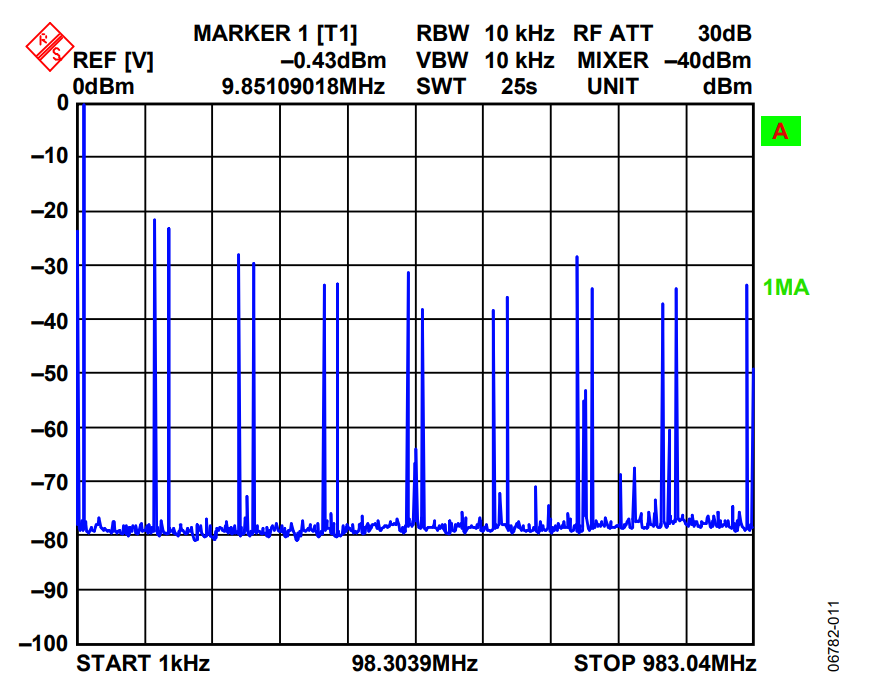
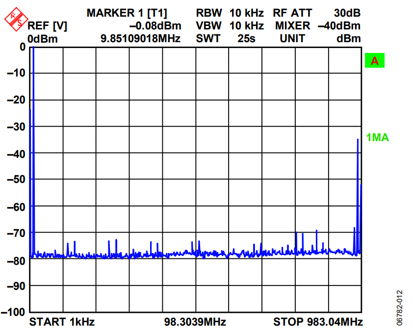
Figure 11 shows an actual spectral plot of the AD9788, with all the DAC images up to 8× the DAC sample rate. PCB board and DAC output parasitics cause this spectrum to differ in places from the ideal DAC function.


If the DAC images are allowed to appear at the input of the quadrature modulator, they are modulated along with the fundamental signal. This can seriously affect the margins with respect to spectral mask requirements. At RF, these DAC images can have as much effect on performance with respect to the spectral mask as any distortion products from the DAC or quadrature modulator. It is therefore necessary to add sufficient filtering between the DAC and quadrature modulator to suppress these images.
The AD9788 provides up to 8× interpolation, which can also be used to suppress the unwanted DAC images. The suppression capability of the AD9788 interpolation filters is shown in Figure 12. Using the interpolation filters can make the design of the DAC reconstruction filter much easier.

Using the AD9788 to Correct for Nonideal Performance of Quadrature Modulators on the IF to RF Conversion
Analog quadrature modulators make it easy to realize single sideband radios. However, there are several nonideal aspects of quadrature modulator performance. Among these analog degradations are
- Gain mismatch. The gain in the real and imaginary signal paths of the quadrature modulator may not be matched perfectly. This leads to less than optimal image rejection because the cancellation of the negative frequency image is less than perfect.
- LO feedthrough. The quadrature modulator has a finite dc referred offset, as well as coupling from the LO port to the signal inputs. These can lead to a significant spectral spurs at the frequency of the quadrature modulator LO.
- Phase mismatch. Because the polyphase filter in the quadrature modulator does not have perfect quadrature over its complete bandwidth, the quadrature of its internal LOs are not perfect. As with gain mismatch, this leads to less than perfect cancellation of the negative frequency image, and less than optimal image rejection.
The AD9788 has the capability to correct for all of these analog degradations. Because these degradations do drift over temperature, if close to optimal single sideband performance is desired, a scheme for sensing these degradations over temperature and correcting for them may become necessary.
Gain Matching and Phase Compensation
Gain matching and phase compensation both affect the total amount of image rejection. Under different conditions (which are difficult to predict), gain or phase compensation may dominate image rejection performance. The user may therefore have to try one of the following techniques for image rejection optimization. When the dominant effect is neutralized, the user may have to perform the other compensation technique to completely suppress the negative frequency image.
In simpler language, if it is found that phase mismatch is dominating the image rejection performance, then the phase compensation on the AD9788 must be used. When the image has been nulled as much as possible using the phase compensation, the user should switch to gain mismatch compensation to completely suppress the image. If it is found that gain mismatch is dominating the image reject performance, then this procedure should start with gain compensation, followed by phase compensation.
Note that LO feedthrough compensation is not dependent on gain or phase compensation; it is a completely separate operation.
Optimizing Gain Matching
Gain matching is achieved by adjusting the values in the DAC gain registers. For the I DAC, these values are in the IDAC Control Register 0x05. For the Q DAC, these values are in the Q DAC Control Register 0x07. These are 10-bit values. To perform gain compensation, simply raise or lower the value of one of these registers by one LSB at a time. Sense if the negative frequency is falling or rising. If the negative frequency image is increasing in amplitude, stop the procedure and try the same adjustment on the other DAC control register. Do this until the image rejection cannot be improved upon by adjusting these registers.
Optimizing Phase Compensation
Phase compensation can also go in one of two directions. The magnitude of the phase compensation is stored in the 10-bit phase correction word in the Phase Control Register 0x0B. The default value of this register is 0. To use the phase compensation, increase the value in the phase correction word one LSB at a time. At the same time, sense whether the negative frequency image is increasing or decreasing. A value of 1023 decimal in the phase correction word is equivalent to −1, so the user may find it necessary to go to 1023 and then decrease this value by one LSB at a time to achieve optimal phase compensation.
LO Feedthrough Compensation
The LO feedthrough compensation is the most complex of all three operations. This is due to the structure of the offset auxiliary DACs. These are current output DACs. To achieve LO feedthrough compensation in a circuit, each of four outputs of these auxiliary DACs must be connected through a 50 Ω resistor to ground and through a 250 Ω resistor to one of the four quadrature modulator signal inputs. The purpose of these connections is to drive a small amount of current into the nodes at the quadrature modulator inputs, therefore adding a slight dc bias to one of the quadrature modulator signal inputs. This is shown in the schematics for the AD9788 evaluation board found in the AD9788 data sheet.
There are four output signals on the auxiliary DACs: two on each auxiliary DAC. One signal is designated p, while the other is n. The magnitude of the auxiliary DAC 1 current is controlled by AUX DAC 1 (Control Register 0x06); the magnitude of the auxiliary DAC 2 current is controlled by AUX DAC 2 Control Register 0x08. These DACs have the ability to source or sink current. This is programmable via Bit 14 in either auxiliary DAC control register. The choice of sinking or sourcing should be made at circuit design time. There is no advantage to programming source or sinking current once a circuit is in place.
The sign bit in each auxiliary DAC control register (Bit 15) controls whether the p side or the n side of the auxiliary DAC is turned on. Only one side of the auxiliary DAC is active at a time. To achieve LO feedthrough compensation, the user should start with the default conditions of the auxiliary DAC sign registers, then increment the magnitude of one or the other auxiliary DAC output currents. While this is being done, the amplitude of the LO feedthrough at the quadrature modulator output should be sensed. If the LO feedthrough amplitude increases, try either changing the sign of the auxiliary DAC being adjusted, or try adjusting the output current of the other auxiliary DAC. It may take some practice before an effective algorithm is achieved. In the lab, using the AD9788 evaluation board, the LO feedthrough can typically be adjusted down to the noise floor, although this is not stable over temperature.
Results of Gain, Phase, and LO Compensation
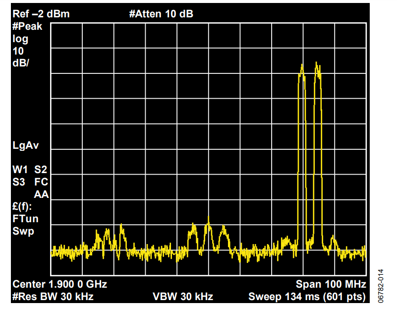
Figure 13 shows the output of the ADL5372 quadrature modulator as configured on the AD9788 evaluation board. In this test, the circuit is synthesizing a CMDA type signal, with two carriers off and two carriers on. This test is typically done to determine how much signal leakage occurs in the spectral regions where the carriers are turned off. The LO feedthrough is significant, as is the amplitude of the negative frequency image. This is an example of typical performance, right out of the box, for these components. In Figure 14, the same circuit is used, but now gain, phase, and LO feedthrough compensation are optimized.


Performance Limitations
This section provides a detailed explanation of other aspects of the quadrature modulator signal chain that may degrade performance.
DAC Noise
Quantization Noise
An in-depth discussion of quantization noise is outside the scope of this application note. Briefly, quantization noise represents the limitation to which an ideal DAC can reproduce a signal. Because a 16-bit DAC can have 216 different output levels, it can reproduce a signal to this accuracy. When the DAC clock and the signal being synthesized are not correlated, the quantization error becomes similar to white noise, and therefore increases the overall noise floor of the DAC output.
Thermal Noise
Thermal noise represents the kT (Boltzmann’s constant × Kelvin temperature) contribution of all of the transistors and other components within the DAC. kT at room temperature is −174 dBm/Hz.
Digital Coupling Noise
Circuitry within the DAC that is switching on and off quickly, such as digital circuitry, can perturb the power supplies and ground distribution, even sending transients onto the substrate itself. Because isolation between digital and analog domains is imperfect, these transients can couple onto the analog section of the DAC. Therefore, a certain amount of noise, often white noise, can be seen on the DAC analog output, due to switching transients in the digital section of the DAC.
In addition, since the primary switching frequency is in the digital section of the DAC clock frequency, spurious components are often seen at multiples of the DAC sample rate. Depending on the technology used and the process geometry, these clock spurs can be as high as −55 dBFS to −60 dBFS, or down to the noise level of the DAC.
Clock spurs due to digital coupling are most troublesome in DACs that offer interpolation. In interpolating DACs, the DAC output sample rate can be 2×, 4×, 8× or a higher multiple of the DAC input data rate. Internal modulators in the DAC can place the input signal anywhere within the spectrum of the DAC, so it is possible (and often a problem) that the input signal is placed near one of these clock spurs. Clock spurs are often high enough to impact spectral masks.
At the time this application note was written, state-of-the-art DACs used in radio transmitters exhibit a total noise floor (combined quantization, thermal, digital noise coupling) in the region of −160 dBm/Hz (spectral noise density). Since kT at room temperature is −174 dBm/Hz, it is unlikely that this will be improved upon significantly in the near future.
DAC Distortion
In simple terms, DAC distortion is a result of the nonlinear transfer function of the DAC. At low output frequencies, distortion is often a function of the DNL and INL of the DAC (refer to DAC data sheets for more information on DNL and INL). At higher frequencies, DAC distortion is a function of the limited linearity of the internal transistors as well as ac parasitic effects.
Quadrature Modulator Noise
Quadrature modulator noise refers to the noise floor of the quadrature modulator. In recent years, advances in the technology of quadrature modulators has followed closely with that of DACs used for radio applications. At the time this application note was written, the input referred noise floor of the best quadrature modulators available was approximately −160 dBm/Hz.
Quadrature Modulator Distortion
As with any other active analog device, the quadrature modulator has a small degree of nonlinear performance. Nonlinearities cause distortion that is more apparent at higher signal levels and higher frequencies. In addition, because it is a mixer, there are distortion components at frequencies of
m × input frequency ± n × LO frequency
A mixer spurious table is useful to determine possibilities for intermodulation distortion.
著者
