AN-2547: Providing Fixed Power Gain at the Output of an IQ Modulator
Circuit Function and Benefits
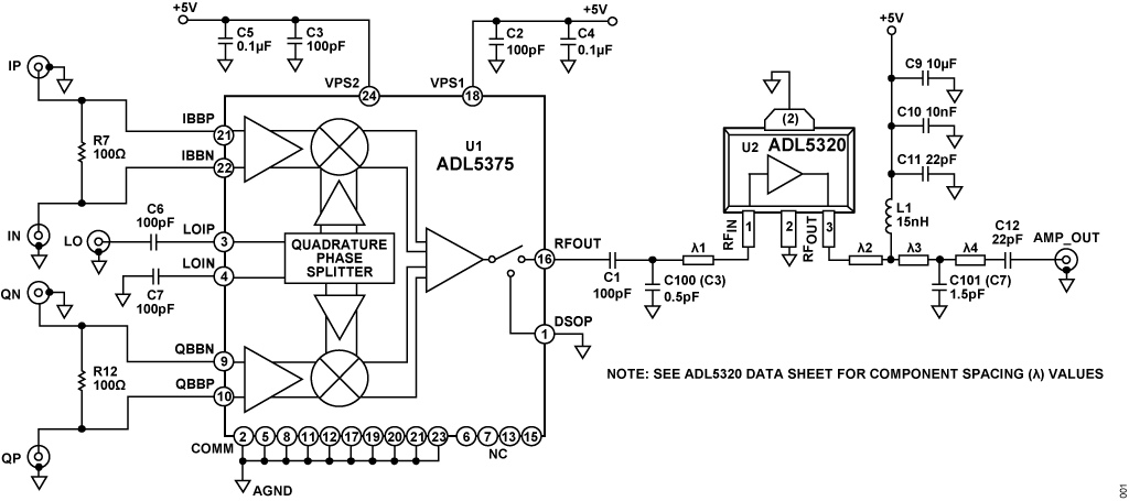
Whether an IQ modulator is used in a direct conversion application or as an upconverter to a first intermediate frequency (IF), some gain is generally applied directly after the IQ modulator. How to choose an appropriate driver amplifier to provide the first stage of gain at the output of an IQ modulator will be described. The devices shown in Figure 1 are the ADL5375 IQ modulator and the ADL5320 driver amplifier. They are well matched from a system performance level; that is, they have equivalent performance so neither device contributes to degradation in the overall performance. Because these devices are well matched in terms of their dynamic ranges, a simple direct connection between the IQ modulator and the RF driver amplifier is recommended without any need for attenuation between the devices.

Circuit Description
The ADL5375 is a general-purpose, high performance IQ modulator. It operates at output frequencies from 400 MHz to 6 GHz. Because of its low noise and wide input baseband bandwidth (3 dB) of 750 MHz, it can be driven by signals with a wide variety of modulations and bandwidths. These input signals can be centered at dc or at a complex IF.
The LO interface to the ADL5375 is a 1XLO type, that is, the output frequency and LO frequency is equal (when the base-band signal is centered at dc).
System Level Calculations and RF Amplifier Choice
In the 1 GHz to 2 GHz frequency range, the ADL5375 has an output compression point (OP1dB) and a third-order compression point (OIP3) of approximately 10 dBm and 25 dBm, respectively. In choosing an RF amplifier to provide gain after the IQ modulator, it is important to choose a device whose input P1dB and input IP3 are equal or a little bit higher than these numbers. Choosing a device with lower specifications results in degraded performance for the cascade while choosing a device whose input P1dB and input IP3 are significantly higher than those of the ADL5375, has little benefit and is likely to needlessly increase the overall supply current of the signal chain.
The ADL5320 is a driver amplifier (RF amplifier that requires external tuning components) that is specified for operation from 400 MHz to 2700 MHz. It consumes 104 mA when operating from a 5 V supply (operation down to 3.3 V is possible with reduced power consumption and performance).
Table 1 shows the output-referred IP3 (OIP3) and P1dB (OP1dB) of the ADL5375 IQ modulator along with the input-referred specifications of the ADL5320 driver amplifier at 1900 MHz. In both cases, there is approximately a 3 dB difference between the outputreferred specifications of the IQ modulator and the input-referred specifications of the amplifier.
| Parameter | ADL5375 (Output Referred) | ADL5320 (Input Referred) |
| IP3 | 24.2 dBm | 28.3 dBm |
| P1dB | 10 dBm | 13 dBm |
Figure 2 shows the simulated cascaded performance of the IQ modulator and drive amplifier at 2140 MHz. This simulation was done using the ADIsimRF Design Tool. It is notable that the 12.3 dB difference between the OIP3 of the modulator (24.2 dBm) and the composite OIP3 (36.5 dBm) is just slightly less than the gain of the ADL5320 driver amplifier, 13.7 dB. This indicates that the driver amplifier has only a very slight effect on the overall OIP3.

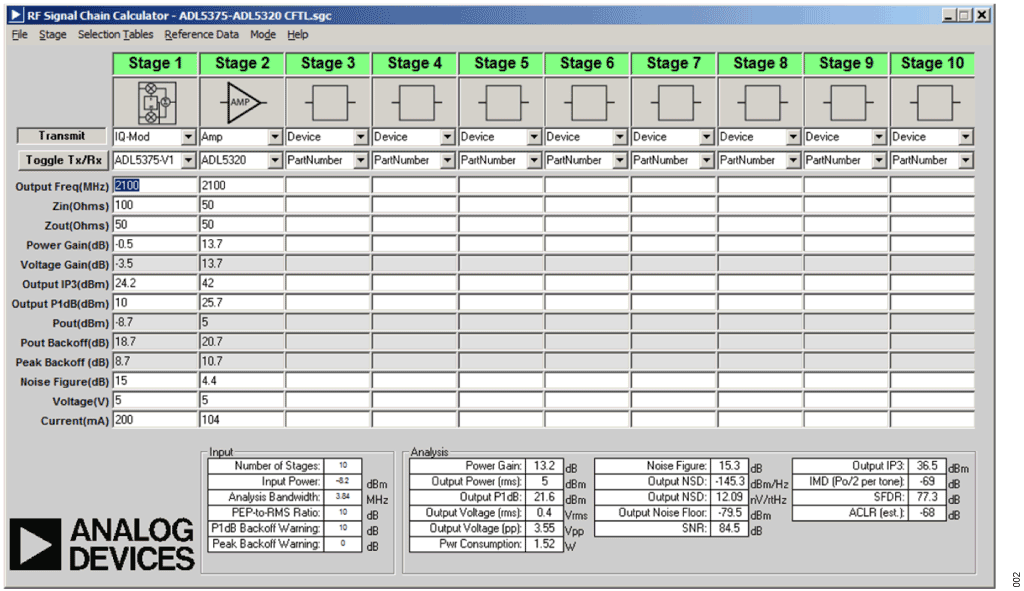
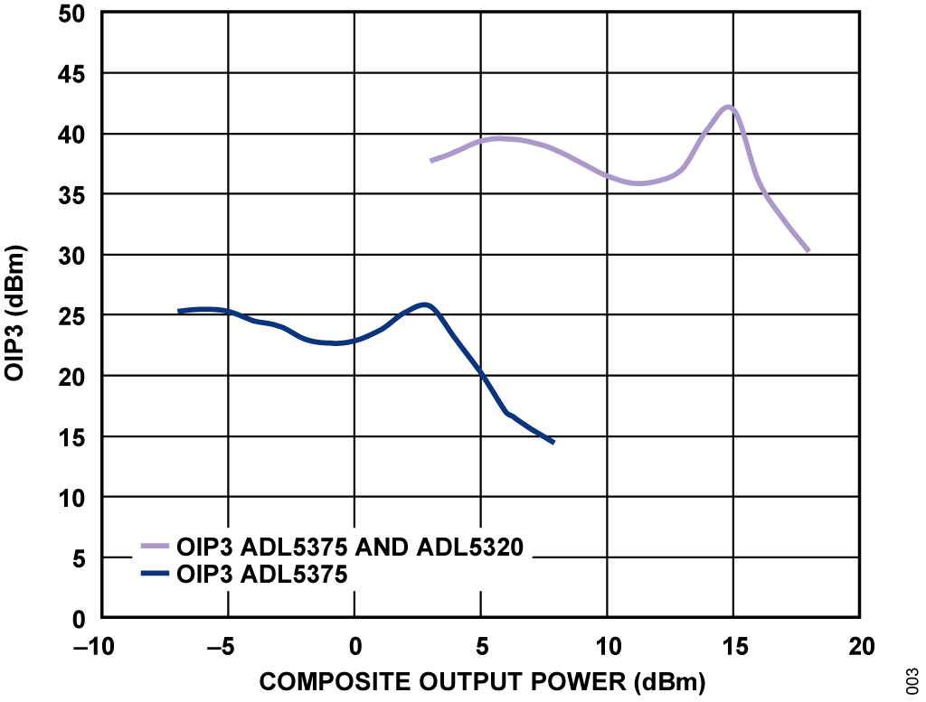
Figure 3 shows a plot of OIP3 vs. output power (POUT) measured at the IQ modulator output and at the output of the composite circuit. The shape of the two OIP3 profiles are quite similar, just shifted in terms of output power and OIP3. This reinforces the idea that the IP3 is only slightly degraded as the signal passes through the RF amplifier

Choosing an Output Power Level
While the circuit achieves OIP3 levels in the 35 dBm to 40 dBm range for output power levels up to 15 dBm, operation is not practical up to these levels, particularly with nonconstant envelope modulation schemes that tend to have relatively high peak-to-average ratios. To understand why, look at the volts-in to power-out transfer function of the circuit and consider the typical drive levels that are available at the input to the IQ modulator.
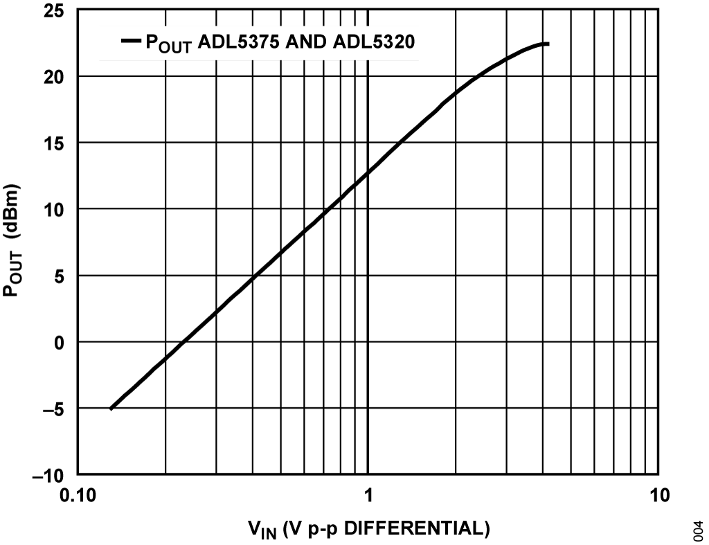
Figure 4 shows the transfer function of the circuit in terms of output power (in dBm) and input voltage (in V p-p) with a CW sine wave, drive signal. An IQ modulator, such as the ADL5375, is driven typically by a dual, current-out, digital-to-analog converter (DAC). Normally, the two current outputs (0 mA to 20 mA nominal) of the DAC are terminated to ground with two 50 Ω resistors and two 100 Ω shunt resistors are placed across each of the IQ inputs. With the DAC running at 0 dBFS, this corresponds to a drive level at the IQ modulator of 1 V p-p or 0.353 V rms (this is neglecting the insertion loss of the low-pass filter that is generally placed between the DAC and the IQ modulator). This results in an output power of approximately 13 dBm.

If it is assumed that the I and Q inputs of the IQ modulator are terminated with 100 Ω as previously discussed, the output power relative to the dBFS drive level of a typical Analog Devices, Inc., DAC can be plotted (see Figure 5). Therefore, a drive level of 0 dBFS corresponds to 1 V p-p, resulting in the same 13 dBm output power previously discussed.
Figure 5 also shows the transfer function of the circuit when the I and Q inputs are not terminated with 100 Ω resistors. Because the resulting DAC voltage drive level is doubled (2 V p-p maximum), the resulting output power is higher by 6 dB for the same DAC drive level.

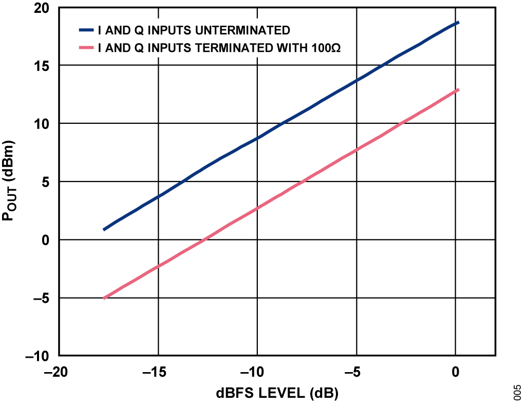
While operation of the circuit without I and Q termination resistors is possible, it does pose some problems for the filter that is usually placed between the DAC and IQ modulator. Because this filter is generally terminated at both ends, it is desirable to have some resistance across the I and Q inputs of the IQ modulator (the unterminated input resistance of these inputs is approximately 60 kΩ). A value that is in the 100 Ω to 1000 Ω range can be used to increase the resulting DAC voltage drive level and corresponding output power. However, take care to design the filter between the DAC and IQ modulator so that it can support different source and load impedances.
As already noted, from Figure 4 and Figure 5, it can be seen that a 1 V p-p sine wave (0 dBFS) is provided an output power of approximately 13 dBm (the I and Q inputs terminated with 100 Ω). In practice, the DAC drive level must be reduced slightly from 0 dBFS to reduce distortion (typically 1 dB to 2 dB). In addition to this, the rms drive level should be lower again by an amount equal to the peak-to-average ratio of the modulation of the carrier. The ratio of peak envelope power (PEP) to rms power is typically in a range from 5 dB for QPSK-like modulation schemes (0 dB in the special case where the modulation is constant envelope) to around 10 dB for higher order QAM-based modulation. Referring to Figure 6, this suggests that output power levels in the 0 dBm to 10 dBm range are feasible.
The adjacent channel power ratio (ACPR) of a single carrier, wideband code division multiple access (WCDMA) signal has become a popular metric for assessing the system level distortion of a circuit (that is, as opposed to an assessment that is solely based on IP3 and IMD levels). Figure 6 shows the measured ACPR of the circuit vs. the output power level. In the case of a WCDMA signal, ACPR is defined as the ratio of the power in the carrier (in a bandwidth of 3.84 MHz) to the power in an adjacent channel (channel spacing = 5 MHz), also measured in a 3.84 MHz bandwidth. The plot also shows an alternate channel power ratio that is the same type of measurement; however, at a carrier offset of 10 MHz.

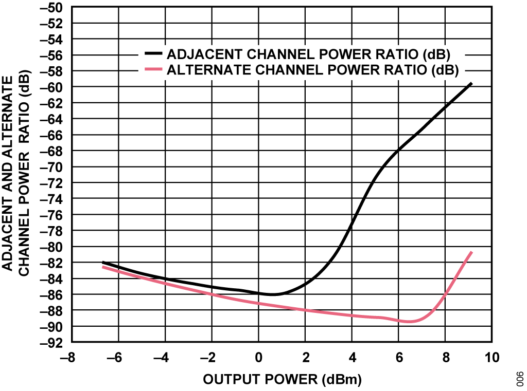
In this case, the signal has a PEP-to-rms ratio of approximately 10 dB (the peak-to-average ratio of a WCDMA signal can vary based on how the carrier is configured and loaded). Based on this plot and the desired level of ACPR, select an output power level in the 0 dBm to 10 dBm range. At power levels less than 0 dBm, the ACPR becomes dominated by the degrading signal-to-noise ratio of the circuit.