AN-1390: Manual Band Selection for PLL Lock Time Reduction
Introduction
The ADRF6820 is a highly integrated demodulator and synthesizer ideally suited for advanced communication systems. It consists of a broadband I/Q demodulator, a fractional-N/integer-N phase-locked loop (PLL), and a low phase noise multicore voltage controlled oscillator (VCO). The multicore VCO covers a fundamental frequency ranging from 2800 MHz to 5700 MHz. The local oscillator (LO) output range is 356.25 MHz to 2850 MHz with the dividers (divide by 2, divide by 4, and divide by 8).
Each VCO core includes multiple overlapping sub-bands to cover a frequency range of several hundred MHz. By setting Bit 0 in Register 0x44 to 0 and Bit 7 in Register 0x45 to 0, the PLL can be programmed to perform a VCO band calibration automatically and enable optimal VCO selection.
The PLL lock process consists of two steps:
- Auto band selection (coarse tuning) via the internal loop. During register configuration, the PLL first switches and configures to the internal loop. An algorithm then drives the PLL to find the correct VCO band.
- Fine tuning via the external loop. The PLL switches to the external loop. The phase detector and charge pump work with the external loop filter as a closed loop to ensure that the PLL locks to the desired frequency. The calibration takes approximately 94,208 phase frequency detector (PFD) cycles; for a 30.72 MHz fPFD, this corresponds to 3.07 ms.
After calibration completes, the feedback action of the PLL causes the VCO to lock to the correct frequency. The lock speed depends on the nonlinear cycle slipping behavior. The total PLL lock time consists of two parts: the VCO band calibration time and the PLL cycle slipping time. The VCO band calibration time is dependent only on the PFD frequency; a higher PFD frequency causes shorter lock times. The PLL cycle slipping time is determined by the implemented loop bandwidth. Cycle slips occur in integer-N/ fractional-N synthesizers when the loop bandwidth is narrow compared to the PFD frequency. The phase error at the PFD inputs accumulates too fast for the PLL to correct and the charge pump temporarily pumps in the wrong direction, dramatically reducing the lock time. If the ratio of PFD frequency to loop bandwidth increases, the cycle slipping also increases, so for a given PFD cycle, increasing the loop bandwidth reduces the cycle flipping time.
Therefore, when using automatic calibration mode, the total lock time may be too long for some applications. This application note proposes a solution that significantly reduces the lock time through manual band selection by doing the following:
- Power up the device with the register initialization sequence detailed in Table 1. By default, the chip works on auto band calibration. Set Register 0x02, Register 0x03, and Register 0x04 according to the required LO frequency.
- Read the lock detect (LD) status bit. High LD indicates that the VCO is locked.
- Read back Register 0x46, Bits [5:0] via the serial peripheral interface (SPI). Assume the value is A and save the register value for all desired LO frequencies in the system on the EEPROM. A table of frequencies and associated register values (see Table 2) is then determined.
- To reduce the LD time, place the ADRF6820 in manual
band selection mode and program the configuration
manually with the data collected in Step 3. The manual
programming procedure is as follows:
- Set Register 0x44 to 0x0001: Disable band calibration algorithm.
- Set Bit 7 in Register 0x45 to 1 to set the VCO band source as saved band information, not from a band calculation algorithm. Program Bits [6:0] in Register 0x45 with the register value recorded in Step 3.
- Select the appropriate VCO frequency range via Register 0x22, Bits [2:0] (see Table 3).
- Update Register 0x02, Register 0x03, and Register 0x04 based on the desired frequency. Register 0x02 sets the divider INT value, which is the integer part of VCO frequency/PFD, Register 0x03 sets the divider FRAC value, which is (VCO frequency/PFD − INT) × MOD, and Register 0x04 sets the divider MOD value, which is PFD/frequency resolution.
- Monitor LD to check if the frequency is locked. For example, PFD = 30.72 MHz and LO = 1600 MHz.
Table 3. VCO Frequency Range LO Selection VCO Frequency Range (MHz) VCO_SEL (Register 0x22 Bits [2:0]) Internal VCO 2850 to 3500 011 3500 to 4020 010 4020 to 4600 001 4600 to 5700 000
Table 4. Manual Band Calibration Register Sequence Register Value Description 0x46 0x0032 Read band calibration value; band calibration value for LO = 1600 MHz 0x44 0x0001 Disable band calibration algorithm 0x45 0x00b2 Setting Bit 7 of Register 0x45 to 1 disables autocal and forces the VCO to use the programmed band value; Bits [6:0] must be loaded with the previously recorded value 0x22 0x2A03 Select appropriate VCO 0x02 0x0034 INT 0x03 0x0066 FRAC 0x04 0x04cd MOD
| Register | Value |
| 0x00 | 0xfeff |
| 0x01 | 0x0041 |
| 0x02 | 0x0003 |
| 0x03 | 0x0020 |
| 0x04 | 0x0000 |
| 0x10 | 0x0c26 |
| 0x20 | 0x000a |
| 0x21 | 0x0082 |
| 0x22 | 0x0800 |
| 0x23 | 0x0002 |
| 0x30 | 0x1106 |
| 0x31 | 0x0900 |
| 0x32 | 0x0000 |
| 0x33 | 0x0a00 |
| 0x34 | 0x0010 |
| 0x40 | 0x000e |
| 0x42 | 0x0000 |
| 0x43 | 0x0002 |
| 0x45 | 0x0000 |
| 0x49 | 0x000f |
| 0x02 | 0x0000 |
| 0x03 | 0x0000 |
| 0x04 | 0x16bd |
| Frequency Point | Register 0x46 |
| f1 | A |
| f2 | B |
Figure 1 and Figure 2 show the test data for the lock detect time with auto band calibration and manual band calibration, respectively. In Figure 2, a high on Line 1 (lock detect) indicates that the PLL is locked. Line 2 (LE), which is the LE pin, is a trigger. Note that the lock detect time must be read from low to high.

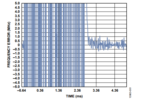


The lock time is approximately 4.5 ms for auto band calibration and approximately 360 μs for manual band calibration. The data was recorded with a 20 kHz loop filter bandwidth and 250 μA charge pump current configuration.
Conclusion
With manual band selection, lock time reduces from a typical value of 4.5 ms to a typical value of 360 μs. For each frequency, first use auto band selection to determine the optimal band value and save it. Because the optimal band value differs from device to device, perform the procedure for each ADRF6820. The VCO band does not need to be updated for temperature variation.
著者
