AD5142
製造中デジタル・ポテンショメータ、デュアル・チャンネル、256ポジション、SPI、不揮発性メモリ
- 製品モデル
- 8
- 1Ku当たりの価格
- 最低価格:$2.12
製品の詳細
- 10kΩと100kΩ抵抗値のオプション
- 抵抗許容誤差:8%(max)
- ワイパー電流:±6mA
- 低温度係数:35ppm/℃
- 広帯域幅:3MHz
- 高速スタートアップ時間:75μs未満
- リニア・ゲイン設定モード
- 単電源動作または両電源動作が可能
- 独立したロジック電源:1.8V~5.5V
- 広い動作温度範囲:-40℃~+125℃
- 3mm×3mmパッケージ・オプション
- 車載アプリケーション用に認定済み
AD5122/AD5142ポテンションメータは、128/256ポジションの調整機能を必要とするアプリケーションに対して、不揮発性のソリューションを提供し、±8%の低い抵抗許容誤差と、Ax、BxおよびWxピンでの電流密度は最大で±6mAの保障を提供します。
この低い抵抗許容誤差と低い公称温度係数は、オープン・ループのアプリケーションを簡素化し、マッチングの許容誤差を重視するアプリケーションにも適します。
リニア・ゲインの設定モードでは、デジタル・ポテンショメータの端子間、RAWとRWB、の抵抗をそれぞれ独立してプログラムすることが可能ですので、非常に高精度な抵抗マッチングを得ることができます。
広い帯域幅と低いTHD(総合高調波歪)は、AC信号に対する最適な性能を得ることがでるので、この製品はフィルタ設計に最適となります。
抵抗アレイの末端のワイパー抵抗は僅か40Ωと低いため、ピンtoピンの接続も可能です。
ワイパーの値は、SPI互換のデジタル・インターフェースを通して設定することができます、またこのインターフェースはワイパー・レジスタとEEPROMの内容をリードバックするためにも使えます。
AD5122/AD5142は、3mm×3mmの16ピンLFCSPパッケージと16ピンTSSOPパッケージを採用しています。これらの製品は、拡張工業用温度範囲-40℃~+125℃で動作が保証されています。
アプリケーション
- 携帯用機器のレベル調整
- LCDパネルの輝度とコントラストの調整
- プログラマブル・フィルタ、遅延、時定数
- プログラマブル電源電圧
ドキュメント
データシート 2
ユーザ・ガイド 1
アプリケーション・ノート 2
| 製品モデル | ピン/パッケージ図 | 資料 | CADシンボル、フットプリント、および3Dモデル |
|---|---|---|---|
| AD5142BCPZ10-RL7 | 16-Lead LFCSP (3mm x 3mm w/ EP) | ||
| AD5142BCPZ100-RL7 | 16-Lead LFCSP (3mm x 3mm w/ EP) | ||
| AD5142BRUZ10 | 16-Lead TSSOP | ||
| AD5142BRUZ10-RL7 | 16-Lead TSSOP | ||
| AD5142BRUZ100 | 16-Lead TSSOP | ||
| AD5142BRUZ100-RL7 | 16-Lead TSSOP | ||
| AD5142WBCPZ10-RL7 | 16-Lead LFCSP (3mm x 3mm w/ EP) | ||
| AD5142WBRUZ10-RL7 | 16-Lead TSSOP |
| 製品モデル | 製品ライフサイクル | PCN |
|---|---|---|
|
5 24, 2016 - 16_0097 Correction of Ilogic Maximum and Typical Specifications in the AD5122/AD5142 Datasheet |
||
| AD5142BCPZ10-RL7 | 製造中 | |
| AD5142BCPZ100-RL7 | 製造中 | |
| AD5142BRUZ10 | 製造中 | |
| AD5142BRUZ10-RL7 | 製造中 | |
| AD5142BRUZ100 | 製造中 | |
| AD5142BRUZ100-RL7 | 製造中 | |
|
8 6, 2014 - 13_0223 Assembly and Test Transfer of Select 2x3mm and 3x3mm LFCSP Products to STATS ChipPAC China |
||
| AD5142BCPZ10-RL7 | 製造中 | |
| AD5142BCPZ100-RL7 | 製造中 | |
|
4 5, 2021 - 21_0035 Amkor Philippines as an Alternate Site for TSSOP_4.4 |
||
| AD5142BRUZ10 | 製造中 | |
| AD5142BRUZ10-RL7 | 製造中 | |
| AD5142BRUZ100 | 製造中 | |
| AD5142BRUZ100-RL7 | 製造中 | |
これは最新改訂バージョンのデータシートです。
ソフトウェア・リソース
必要なソフトウェア/ドライバが見つかりませんか?
ドライバ/ソフトウェアをリクエストツールおよびシミュレーション
IBISモデル 1
評価用キット

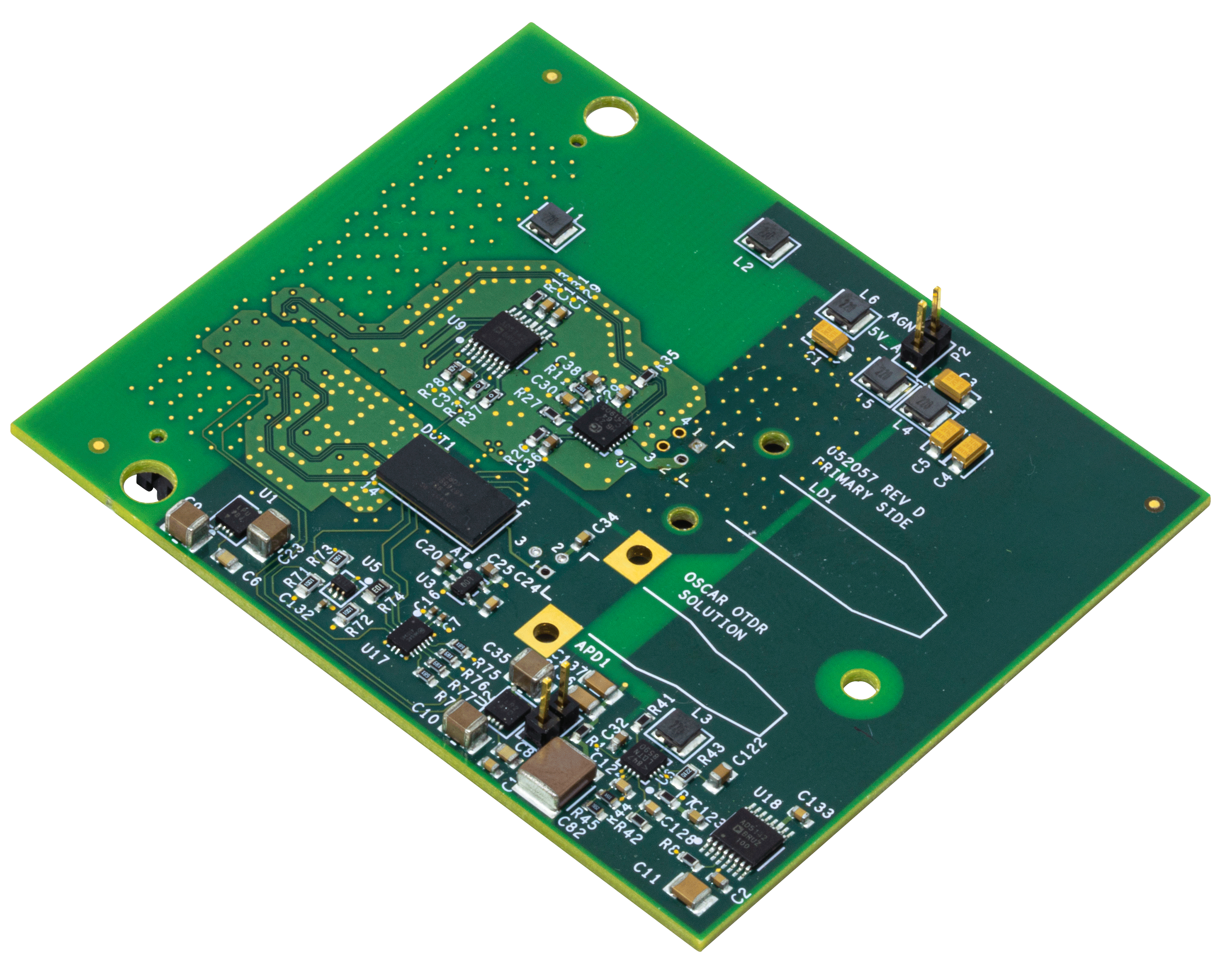
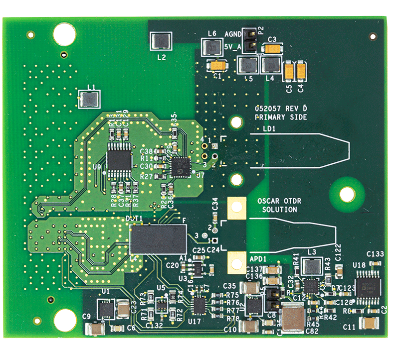
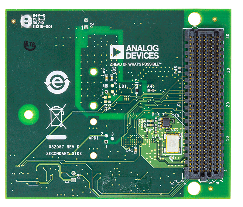
AD5142 Evaluation Board
資料
ソフトウェア
Evaluation System for the ADA4355