Versatile Current Sense Amplifiers Offer Rail-to-Rail Input, 150°C Operating Temperature
Versatile Current Sense Amplifiers Offer Rail-to-Rail Input, 150°C Operating Temperature
Mar 1 2008
Introduction
Fast and accurate current measurement is required in an increasing number of electronics subsystems. The list of applications that call for current sensing includes diagnostic system assessment, fault detection, load protection and scaling, battery “gas gauge” monitoring, and impending component failure detection, to name just a few. The challenge is that there is no one-size-fits-all solution for current measurement. For example, protection circuits often emphasize measurement speed, while battery applications usually emphasize accuracy and low power. Nevertheless, design time can be reduced by using an accurate current measurement amplifier with features suited to the task at hand, such as the latest members of Linear Technology’s current sense amplifier family, the LT6105, LT6106 and LT6107.
The LT6105 is distinguished by its rail-to-rail inputs. It is a perfect fit for automatic test equipment (ATE) systems and other systems that use a combination of fixed voltage supplies and programmable or switched supplies. The LT6105 features an input voltage range of –0.1V to 44V that is independent of the power supply voltage. The supply voltage for the LT6105 can be obtained from any convenient source within the supply range of 2.85V to 36V. For instance, a programmable supply with an output of 0V to 24V can be monitored while the LT6105 is powered by a fixed 5V supply.
The LT6106 is distinguished by ease-of-use and accuracy in single supply environments. Just add two resistors and tie the supply to the sense resistor, and the device is configured to measure currents in supplies from 2.7V to 36V. Input offset voltage is a low 250µV and the power supply rejection of 106dB makes the accuracy almost independent of supply.
The LT6107 is functionally identical to the LT6106, but provides guaranteed performance and specifications at junction temperatures up to 150°C. This suits it to under hood automotive and some industrial applications that can exceed 125°C for relatively short periods of time. Input offset voltage is less than 400µV over the entire temperature range of –40°C to 150°C. As with the LT6106, two external resistors set the amplifier gain.
Table 1 summarizes the guaranteed performance of the LT6105, LT6106 and the LT6107.
| Parameter | LT6105 25°C |
LT6106 25°C |
LT6107 –40°C to 150°C |
| Input Voltage Range | –0.3V to 44V | 2.7V to 36V | 2.7V to 36V |
| Supply Voltage Range | 2.85V to 36V | 2.7V to 36V | 2.7V to 36V |
| VOS | 300µV/1000µV* | 250µV | 400µV |
| Maximum Differential Input Voltage | 44V | 0.5V | 0.5V |
| CMRR | 95dB | N/A | N/A |
| PSRR | 100dB | 106dB | 106dB |
| Gain Error | ±1%/±2.5%* | –0.65% to 0% | –0.65% to 0% |
| Output Current | 1mA | 1mA | 1mA |
| Supply Current | 340µA | 95µA | 125µA |
| Package | MS8, DFN | TSOT-5 | TSOT-5 |
| * Input common mode voltage = 12V, 0V | |||
Flexible Gain Setting
The LT6105, LT6106 and LT6107 use traditional external gain-setting resistors. This is actually an important feature in a current sense amplifier. Most current sense applications require a very small maximum sense shunt voltage (to minimize power loss), which must be amplified to match either a very specific comparator threshold or ADC input voltage span. The ability to carefully control the gain is paramount to optimize performance. Figures 1 and 2 show typical applications of the LT6106 and LT6105.

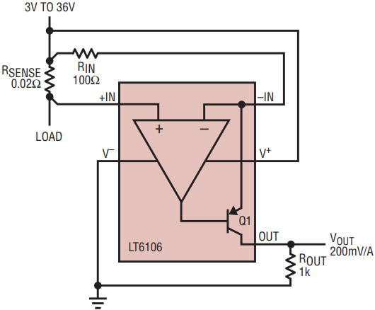
Figure 1. Typical current sense application using the LT6106. Sense resistor is 20mΩ and gain is 10, so transfer function is VOUT/ILOAD = 0.2V/A.

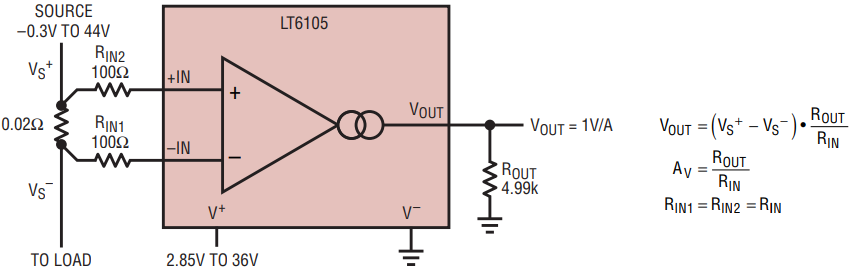
Figure 2. Typical LT6105 connection. Sense resistor is 20mΩ and gain is 50, so the transfer function is VOUT/ILOAD = 1V/A. Note the wide input source.
LT6106, LT6107 Theory of Operation
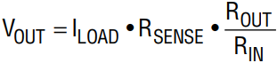
Referring to Figure 1, the current to be measured, ILOAD, passes through a sense resistor RSENSE, resulting in a voltage drop of VSENSE. Feedback from the amplifier causes a current to flow in RIN and Q1 such that the amplifier inputs are equal, V–IN = V+IN. The current in Q1 also flows through ROUT. The output voltage is therefore proportional to the load current and is given by
The overall accuracy graph shown in Figure 3 combines the effects of gain error and input offset voltage to create a worst-case error band for the application circuit in Figure 1. A slight negative gain error, typically –0.25%, is due to the finite current gain of the PNP.

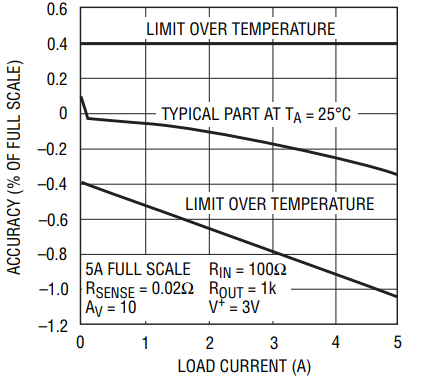
Figure 3. Measurement accuracy vs load current for the LT6106 and LT1607.
The LT6105: Robust and Easy to Use
The LT6105 tolerates negative voltages on its inputs of up to –9.5V. In addition, it can also be used to sense across fuses or MOSFETs as shown in Figure 4. The LT6105 has no problem when the fuse or MOSFET opens because it has high voltage PNP’s and a unique input topology that features full high impedance differential input swing capability to ±44V. This allows direct sensing of fuse or MOSFET voltage drops, without concern for an open circuit condition in the fuse or MOSFET.

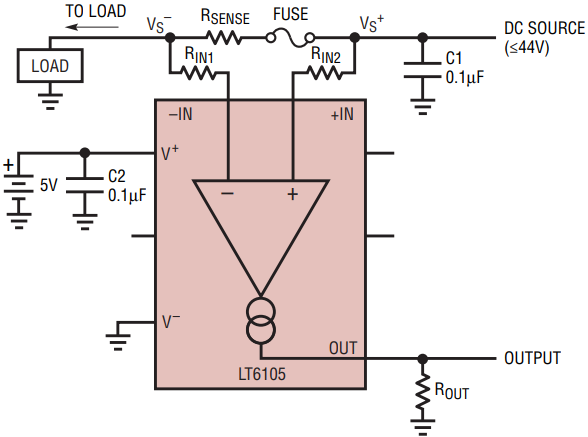
Figure 4. The LT6105 can monitor across a fuse or switch. It’s inputs are undamaged even when split wide apart, and current is limited to about 3mA.
Another benefit of the LT6105 is that you can leave it connected to a battery even when it is unpowered. When the LT6105 loses power, or is intentionally powered down, both sense inputs remain high impedance. In fact, when powered down, the LT6105 inputs actually draw less current than when powered up. Powered up or down, it represents a benign load.
The LT6105 extends the current sense measurement concept used in the LT6106 (and others) to accommodate an input voltage range that includes ground. For both the LT6105 and LT6106, the voltage developed across a sense resistor is translated into a current that appears in the output pin. The voltage gain is set by the ratio of the input and output resistors, (ROUT/RIN). The wide input range in the LT6105 is obtained by the use of two feedback paths to the input pins.
Referring to Figure 5, when the input voltage VS+ is between 0V and 1.6V, devices Q1, Q2, and Q3 are active and devices Q4–Q7 are off. Feedback from the amplifier causes the current to flow in Q1, which equalizes the amplifier input voltages. Devices Q1 and Q3 are matched, so the collector current of Q3 will equal the collector current of Q1. The output voltage is then
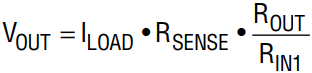

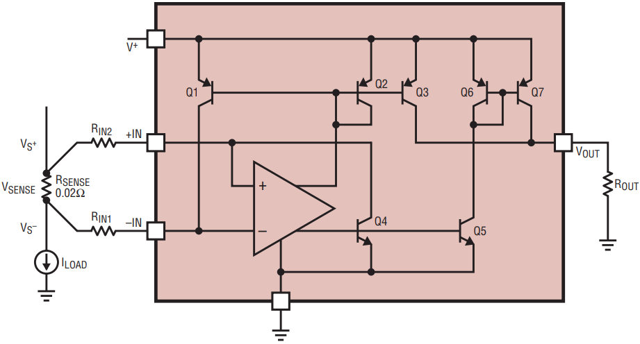
Figure 5. Block diagram of the LT6105.
When the input voltage VS+ is greater than 1.6V, devices Q4, Q5, Q6, and Q7 are active and devices Q1–Q3 are off. Again, feedback from the amplifier causes the current to flow in Q4 which equalizes the amplifier input voltages. The current in Q4 is mirrored to the output through the matching of Q4 to Q5 and Q6 to Q7. The output voltage for this mode is given by

LT6105 Application: Solenoid Current Monitor
The large input common mode range of the LT6105 makes it suitable for monitoring currents in quarter, half, and full bridge inductive load driving applications. Figure 6 shows an example of a quarter bridge. The MOSFET pulls down on the bottom of the solenoid to increase the solenoid current. It lets go to decrease current, and the solenoid voltage freewheels around the Schottky diode. Current measurement waveforms are shown in Figure 7. The small glitches occur due to the action of the solenoid plunger, and this provides an opportunity for mechanical system monitoring without an independent sensor or limit switch.

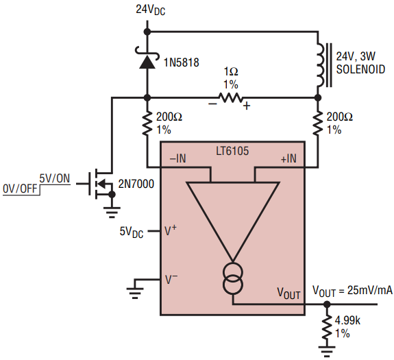
Figure 6. Simplest form of solenoid driver. The LT6105 monitors the current in both on and freewheel states. Lowest common mode voltage is 0V, while the highest is 24V plus the forward voltage of the Schottky diode. See waveforms, Figure 7.

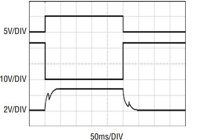
Figure 7. Waveforms for solenoid driver. Top trace is the MOSFET gate, with high on. Middle trace is the bottom of the solenoid/inductor. Bottom trace is the LT6105 output, representing solenoid current at 80mA/DIV. Glitches are useful indicators of solenoid plunger movement.
Figure 8 shows another solenoid driver circuit, a high side drive approach with one end of the solenoid grounded and a P-Channel MOSFET pulling up on the other end. In this case, the inductor freewheels around ground, imposing a negative input common mode voltage of one Schottky diode drop. This voltage may exceed the input range of the LT6105. This does not endanger the device, but it degrades the accuracy. In order to avoid exceeding the input range, pullup resistors may be used as shown.

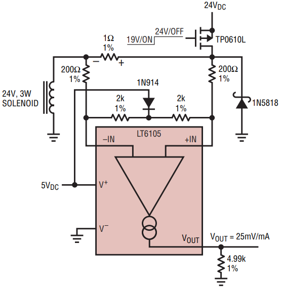
Figure 8. Similar circuit to Figure 6 but with solenoid grounded, so freewheeling forces inputs negative. Providing resistive pullups keeps amplifier inputs from falling outside of their accurate input range.
LT6105 Application: Supply Monitor
The input common mode range of the LT6105 also makes it suitable for monitoring either positive or negative supplies. Figure 9 shows one LT6105 applied as a simple positive supply monitor, and another LT6105 as a simple negative supply monitor. Note that the schematics are practically identical, and both have outputs conveniently referred to ground. The only requirement for negative supply monitoring, in addition to the usual constraints of the absolute maximum ratings, is that the negative supply to the LT6105 be at least as negative as the supply it is monitoring.

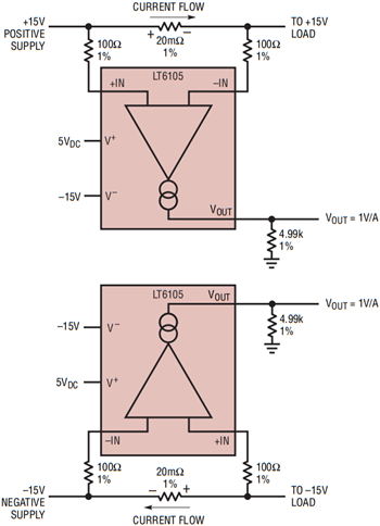
Figure 9. The LT6105 can monitor the current of either positive or negative supplies, without a schematic change. Just ensure that the current flow is in the correct direction.
Conclusion
The LT6105, LT6106, and LT6107 provide simple, flexible solutions to high side (and low side) current sensing. Common to all the parts is the flexibility of external gain setting. The –0.1V to 44V input range of the LT6105 enables the current in switched supplies to be monitored from initial turn-on/turn-off to the steady state value. The LT6106 provides a simple but accurate solution for systems with a single supply. The LT6107 extends the temperature range of current measurements to 150°C.
About The Authors
Glen Brisebois is an applications engineer with the Signal Conditioning Group at Analog Devices in Silicon Valley. He attended the University of Alberta in Canada, achieving bachelor’s degrees in both physics and electrica...
{{modalTitle}}
{{modalDescription}}
{{dropdownTitle}}
- {{defaultSelectedText}} {{#each projectNames}}
- {{name}} {{/each}} {{#if newProjectText}}
-
 {{newProjectText}}
{{/if}}
{{newProjectText}}
{{/if}}
{{newProjectTitle}}
{{projectNameErrorText}}
Latest Media 20