CN0415


Overview
Design Resources
Design & Integration File
- Schematic
- Bill of materials
- Gerber files
- Allegro layout files
- Assembly drawing
Evaluation Hardware
Part Numbers with "Z" indicate RoHS Compliance. Boards checked are needed to evaluate this circuit.
- EVAL-ADICUP3029 ($52.97) ADuCM3029 Arduino Form Factor Compatible Development System
- EVAL-CN0415-ARDZ ($153.01) Robust Soleniod Measurement and Drive System
Product Categories
Markets and Technologies
Parts Used
Documentation & Resources
-
CN0415 User Guide3/13/2019WIKI
-
CN0415: Robust, Closed-Loop Control and Monitoring System for Solenoid Actuators (Rev. 0)3/1/2019UNDEFINEDundefined
Circuit Function & Benefits


The simplified circuit diagram shown in Figure 1 is a robust solution for accurately and efficiently driving proportional and two-state solenoid actuators. Applications include motion control, latches, clamps, brakes, clutches, proportional gas valves, and proportional liquid valves.
In two-state solenoid applications, this circuit provides accurate, closed-loop current control, allowing low voltage solenoid use over a wide range of supply voltages. Initial pull-in current, pull-in time delay, and hold current are independently adjustable, greatly reducing power consumption in applications in which the solenoid is continuously energized.
For proportional valve applications, this circuit provides a complete driver solution; pulse-width modulation (PWM) duty cycle and frequency can be directly controlled by an external PID controller, and a dither current with programmable frequency and amplitude can be enabled to reduce mechanical stiction.
A high voltage, current shunt monitor measures the instantaneous solenoid current, which is then digitized for software control. Full-scale current is 2.0 A, which can be modified by changing a single shunt resistor. A redundant overcurrent limit circuit continuously monitors solenoid current, latching off and notifying the controller when tripped, protecting the solenoid in the event of hardware or software faults. Power entry circuitry includes protection for overvoltage events up to 60 V and reverse voltage to −40 V, with power being enabled within a valid window from 6 V to 24 V only, ensuring predictable operation over supply transient conditions, for instance, undervoltage during cold cranking or overvoltage resulting from a load dump.
Circuit Description
Fundamentals of Solenoid Actuator
The electrical characteristics of typical solenoid actuators are primarily inductive and resistive. A voltage applied across a solenoid actuator causes a current to ramp with an initial slope of voltage/inductance (V/L), eventually reaching a steady state current of voltage/resistance (V/R). This V/L/R characteristic is the primary reason why current does not immediately reach a maximum level when a solenoid is energized. The solenoid stores energy in the form of a concentrated magnetic field. A magnetic field is generated around the conductor wire whenever there is a current flow present in the wire. The magnetic field becomes concentrated with the wire wound into a coil, such as in a solenoid. This electromagnet can control a mechanical valve through an electrical signal. PWM can be used to reduce the effective voltage applied to a solenoid (and hence control the current of the solenoid), with the effective voltage being expressed as follows:
V × Duty Cycle
In general, solenoid basically consist of an electrical coil wound around a cylindrical tube with a ferromagnetic actuator or plunger that is free to move or slide in and out of the body of the coil, as shown in Figure 2.


The force on the armature of the solenoid is approximately proportional to the current and inversely proportional to the square of the gap between the armature and core. Thus two-state solenoids typically have a return spring with a linear response (or no return spring), whereas proportional solenoids use a nonlinear spring such that armature displacement is proportional to solenoid current. Armature movement does affect solenoid current (as shown in Figure 3), but this movement typically does not have a significant impact on circuit operation.


Current Sense
Measuring solenoid current is a particularly challenging task, especially when PWM techniques are involved. This system uses a topology consisting of a high-side current sense with a low-side switch. In this case, the PWM control switch is ground referenced. The inductive load (solenoid) is tied directly to the power supply, and a resistive shunt is placed between the switch and the load (see Figure 4).


An advantage of placing the shunt on the high side is that the entire current, including the recirculation current, can be measured because the shunt remains in the loop when the switch is off. In addition, diagnostics can be enhanced because short circuits to ground can be detected with the shunt on the high side.
In this configuration, the common-mode voltage of the sense resistor swings between ground (when the MOSFET is on) and 0.4 V above the input supply (when the MOSFET is off). The AD8210, which operates at a single-supply, is a difference amplifier that is ideal for amplifying small differential voltages in the presence of large common-mode voltages. The operating input common-mode voltage range extends from −2 V to +65 V when powered by a single 5 V supply. The gain of the amplifier is 20V/V, set by internal precision and low drift resistors that result to a 5 V output voltage from a maximum input full-scale range of 250 mV-peak. Calculate the output of the AD8210 as shown in Equation 1.

The full-scale design current is 2 A; a 0.1 Ω sense resistor results in a 4 V output, slightly lower than the 4.096V full-scale input of the ADC.
The sense resistor power rating must support the full-scale current. For a 2 A design current, the dissipation is

A 1 W resistor is used in this design, giving a 2.5 safety margin.


The AD8210 −3 dB bandwidth is 450 kHz, providing adequate bandwidth for PWM frequencies up to 45 kHz. The AD8210 output is directly monitored by an overcurrent protection circuit. Shown in Figure 5 is a first-order low-pass filter at the input of the AD8210 that helps reduce the ripple of the current sense signal before being digitized. The cutoff frequency, f−3 db, is determined by Equation 3.

where:
RFILTER = 50 Ω and R5
CFILTER = 4.7 μF and C2, resulting in a cutoff frequency of 677 Hz
The signal path has provision for an additional RC low-pass filter that is bypassed by default.
ADC Data Acquisition
The solenoid current is digitized by an LTC2312-14, a 14-bit, 500 ksps sampling ADC. The LTC2312-14 has an integrated voltage reference that automatically optimizes the input range to 2.048 V or 4.096 V for power-supply voltages of 3.3 V or 5 V, respectively.
The internal reference has low impedance (1 Ω typical), allowing it to be used for other circuitry without requiring additional buffering. EVAL-CN0415-ARDZ uses the reference of the ADC to accurately set the overcurrent threshold, and can optionally be used to set the offset of the current monitor to half scale. For applications with less stringent accuracy requirements, the solenoid current can be connected to the analog input of the microcontroller.
FET Driver
Pulse-width modulation (PWM) is a method of varying a dc supply voltage by switching the supply fully on and fully off, varying the ratio of on time to off time. The ratio of on time to the period (sum of on time and off time) is the duty cycle of the PWM signal
At 50% duty cycle the voltage is on for 50% of the time period and off for the remaining 50%. Therefore, the time average voltage is 50% of the dc input supply voltage, and the current through the solenoid is proportionally less. Furthermore, the current to the solenoid is only 50% of maximum current. Whereas the frequency (reciprocal of the period) of a PWM signal is variable in some applications, it is often set to a fixed value. There is often a range of frequencies that work for a given application, with the following criteria:
- The PWM frequency should be much greater than the mechanical response of the system/actuator
- The PWM frequency should be low enough to prevent excessive switching losses
The EVAL-ADICUP3029 platform board used with CN-0415 has a built-in PWM generation peripheral. The output of the controller is not capable of driving the switching MOSFET directly—the logic high voltage of 3.3 V is not high enough to fully enhance the MOSFET, and the drive strength is not sufficient to rapidly switch the MOSFET, resulting in increased power dissipation as the MOSFET transitions through saturation.
An LTC4441 N-MOSFET gate driver solves these issues by providing a gate drive voltage of up to 8 V at a current of 6 A, rapidly switching the MOSFET and minimizing losses. The logic input is TTL-compatible and directly interfaces to 3.3 V CMOS logic. A dual-function control input is provided to disable the driver or to force the chip into shutdown mode with <12 µA of supply current. Undervoltage lockout and overtemperature protection circuits disable the driver output when activated.
Overcurrent Protection Circuit
In normal operation, solenoid current is controlled by software. It is prudent to include a failsafe overcurrent circuit in the event of software glitches or malfunctions. Fault detection signals can either be interrupt driven or detected in the proportional integral derivative (PID) loop.
CN-0415 accomplishes this PID control loop by continuously monitoring the AD8210 output with an LT1671 precision comparator with output latch. The overcurrent threshold is set by R14 and R15, which form a resistive divider that is driven by the 4.096V reference of the LTC2312-14 (see Figure 6). Equation 4 is the expression for the trip voltage, which is set to 3.41 V by default, corresponding to a solenoid current of 1.7 A.

In the event of an overcurrent condition, the comparator output disables the LTC4441 and latches. The output is also routed to a microcontroller general-purpose input/output (GPIO) pin such that software can detect this condition and act accordingly. When the fault has been cleared, the comparator can be reset by a rising edge at the gate of Q3. In Figure 6, a rising edge detector is used instead of a level sensitive reset, because a software fault can leave the reset signal at a high level.)


Power Supply and Protection
An LTC4367 overvoltage, undervoltage, and reverse supply protection controller provides robust power input protection. The LTC4367 protects applications where power supply input voltages may be too high, too low, or even negative, by controlling the gate voltages of a pair of external N-channel MOSFETs to ensure that the output stays within a safe operating range. A 32 ms turn-on delay also blocks 50 Hz or 60 Hz ac. The LTC4367 withstands voltages between –40 V and +100 V and has an operating range of 2.5 V to 60 V, consuming only 70 μA in normal operation.
The LTC4367 includes two accurate comparators to monitor for overvoltage and undervoltage conditions at VIN. If the input supply rises above the user adjustable overvoltage threshold, the gate of the external MOSFET is quickly turned off, thus disconnecting the load from the input. Similarly, if the input supply falls below the user adjustable undervoltage threshold, the gate of the external MOSFET is quickly turned off.
The overvoltage (OV)/undervoltage (UV) resistor values are determined with the following parameters shown in Table 1.
| Parameter | Value |
| VOS | 3 mV |
| ILEAK | 10 nA |
| UVTH | 2.2 V |
| OVTH | 24 V |
The relevant data sheet formulas are shown in Equation 5 through Equation 7

Resulting in the values for the divider listed in Table 2.
| Resistor | Value |
| R4 | 272.5 kΩ |
| R5 | 27.5 kΩ |
| R8 | 1.02 MΩ |
Industrial, automotive, and battery-powered applications often subject circuits to various transient situations, including load dump and cold crank conditions. Load dump occurs in an automotive application if the battery is disconnected while being charged by the alternator, and results in a rapid increase in supply voltage. Cold crank occurs when starting an engine (or other high load condition), producing a voltage drop in the battery (which is exacerbated at low temperatures). An LT3433 current mode switching regulator handles these situations, as it provides both step-up and step-down regulation using a single inductor. The circuit operates over a 4 V to 60 V input voltage range, making it suitable for use in various wide input voltage range applications.


Figure 7 shows a high voltage step-up/stepdown dc-to-dc converter switching regulator circuit that provides a regulated 5 V voltage output supply to the amplifiers and to the digital converters.
System Power Dissipation
The estimated quiescent current consumed by the system is approximately 13 mA or around 180 mW, as listed in Table 3 comparable to the simulated current consumed by the system where the voltage input supply, that can range from 6 V to 24 V, was set at 12 V.
| IC Devices | VSUPPLY (V) | IQ1 (A) | Watts (W) |
| AD8210 | 5 | 0.002 | 0.01 |
| LTC4441 | 24 | 0.006 | 0.144 |
| LT1671 | 5 | 0.001 | 0.005 |
| LTC4367 | 24 | 0.00009 | 0.00216 |
| LT3433 | 5 | 0.00094 | 0.0047 |
| LTC2312-14 | 5 | 0.003 | 0.015 |
| Total | N/A2 | 0.01303 | 0.18086 |
| 1 IQ means quiescent current. 2 N/A means not applicable. |
|||
Digital PID Control
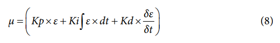
A PID control loop allows the solenoid current to be accurately controlled, compensating for variations in supply voltage and coil resistance. This mode of operation allows for optimum drive current for two-state solenoids, minimizing power dissipation. An additional function allows a higher initial pullin current to be applied for a short time, after which current drops back to a lower hold current. For a digital implementation of a PID controller, the standard form of the PID controller must be discretized. The discretized PID controller is expressed in Equation 8 where Kp, Ki and Kd should be first tuned with the right values.
For complete information and details regarding software routine, refer to the CN-0415 Software wiki.
Common Variations
A system that requires low offset drift and operates at a lower voltage input for a current sense amplifier, an AD8418 can be used as an alternative forAD8210. The AD8418 amplifier has a 0.1 μV/°C offset drift and can operate from 2.7 V to 5.5 V, making the AD8418 more compatible for portable applications.
Circuit Evaluation & Test
The following section outlines testing procedures and the gathering of the results for the CN-0415 circuit design. For more information hardware and software setup, visit the CN-0415 User Guide for complete details.
Equipment Needed for Test
- PC with a USB port and Windows® 7 or above
- EVAL-CN0415-ARDZ circuit evaluation board
- EVAL-ADICUP3029 evaluation platform or equivalent interface
- CrossCore® Embedded Studios (interactive development environment (IDE))
- Power supply: 6 V to 12 V bench power supply or equivalent
Getting Started
Load the sample code onto the CrossCore Embedded Studios IDE by following the instructions in the CN-0415 User Guide.
Functional Block Diagram
Figure 8 shows the functional block diagram of the test setup. The test requires a voltage supply ranging from 6 V to 25 V and a solenoid actuator as the system load.


Setup
Connect the EVAL-CN0415-ARDZ by mounting it atop the EVAL-ADICUP3029 board using the Arduino-compatible headers with their corresponding headers, as shown in Figure 9.


Test
With the sample code built and loaded onto the EVALADICUP3029 and the EVAL-CN0415-ARDZ mounted with the solenoid actuator connected, the device communicates with the PC, allowing codes to be written to the device via the UART. Test the circuit by using the different command lines available for evaluation purposes, such as the PWM frequency, the duty cycle, and also its current load for the actuator. For complete information and details regarding test setup and how to use the software and hardware combined, refer to the CN-0415 User Guide. More information regarding the EVALADICUP3029 board is available in the EVAL-ADICUP3029 User Guide.
The system was tested using a 12 V solenoid actuator with an inductance of 20 mH and a dc resistance of 12 Ω. The actuator used is a dc push-pull solenoid. It operates at a 12 V supply and can produce a 6 newton (N) at 50% duty cycle. Note that for the purposes of testing electrical performance, an inductor can be used as an alternative load. Figure 10 shows the actual voltage output from the AD8210.


PWM Driver Accuracy Test
The PWM signal is generated from the microcontroller and passes through several active devices that distort the duty cycle to some degree. Figure 11 shows a graph of measured PWM error vs. duty cycle for several PWM frequencies. The results show that distortion induced error is more apparent at high PWM frequencies and low duty cycle. This effect is less important in the closed-loop current control mode of operation, as the precision feedback from the ADC corrects for this error.


Closed-Loop System Test
The system was tested in closed-loop current mode, as well. In the closed-loop current mode of operation, errors are dominated by elements in the feedback path: the current sense resistor, current sense amplifier, and ADC with internal reference. Errors due to PWM distortion, variations in supply voltage, and temperature coefficient of the solenoid coil are all corrected.


The full scale error vs. programmed current for various PWM frequencies is shown in Figure 12. The gain error ranges up to about 2.8 mA with an offset up to 3 mA (which is about 0.5% of full scale). The example software includes a calibration routine, allowing the initial errors to be calibrated out, leaving a residual error of less than 1 mA (about 0.16% of full scale).