AN-2572: A Robust, Low Power, Battery Monitoring Circuit Front End
Circuit Function and Benefits
The circuit shown in Figure 1 is a robust battery monitoring front end designed for environments where transients are likely to occur, such as in industrial or process automation environments. The circuit uses the ADG5408 8-channel CMOS multiplexer followed by the AD8226 instrumentation amplifier to provide accurate voltage monitoring of individual cells at low power and low cost, and requires no additional external transient protection circuitry.
Transient overvoltage conditions may cause traditional CMOS switches to experience latch up. In junction isolation technology, the N- and P-wells of the PMOS and NMOS transistors form a parasitic silicon-controlled rectifier (SCR) circuit. An overvoltage condition triggers this SCR, causing a significant amplification of current that, in turn, leads to latch-up. Latch-up is an undesirable, high current state that can lead to device failure and can persist until the power supply is turned off.
Latch-up can occur if either the input or the output pin voltage exceeds the supply rail by more than a diode drop, or by improper power supply sequencing. If a fault occurs on the channel, and the signal exceeds the maximum rating, the fault can trigger the latch-up state in an typical CMOS part.
During circuit power up, it is also possible for voltages to occur on inputs before power is applied to the CMOS switch, especially if multiple supplies are used to power the circuit. This condition may exceed the maximum rating of the device and trigger a latch-up state.
The two multiplexers and the instrumentation amplifier (IA) used in this design have robust inputs. The ADG5408 is a high voltage 8:1 multiplexer that is latch-up proof. The trench isolation technology used in the fabrication of the ADG5408 prevents the latch-up state and reduces the need for external protection circuitry. Latch-up proof does not guarantee overvoltage protection and only means the switch does enter the high current SCR mode. The ADG5408 also has an electrostatic discharge (ESD) rating of 8 kV human body model (ANSI/ESDA/JEDEC JS-001-2010).
The AD8226 is a low cost, low power, instrumentation amplifier with robust inputs and can handle input voltages up to 40 V from the opposite supply rail, while restricting the output to within the rails. For instance, with ±18 V supplies, the positive or negative input of the AD8226 can swing between ±22 V with no damage. All inputs of the AD8226 are protected against ESD with internal diodes.
Circuit Description


Battery monitoring systems (BMS) require the individual voltage across each battery in a battery stack to assess the state of charge (SOC) and state of health (SOH) of the battery. By multiplexing the terminals of a stack of batteries with two multiplexers, as shown in Figure 1, the voltage across each battery can be assessed.
One multiplexer is used for the positive terminal and another for the negative terminal. This differential multiplexing allows the use of a single instrumentation amplifier for up to eight channels. The amplifier then removes the common-mode voltage from each of the batteries for use by the BMS.
The ADG5408 has a low on-resistance per channel, typically 13.5 Ω, and a maximum of 22 Ω over temperature. With a maximum of 2 nA input offset current, there is a maximum of 44 nV error voltage across the channel resistances.
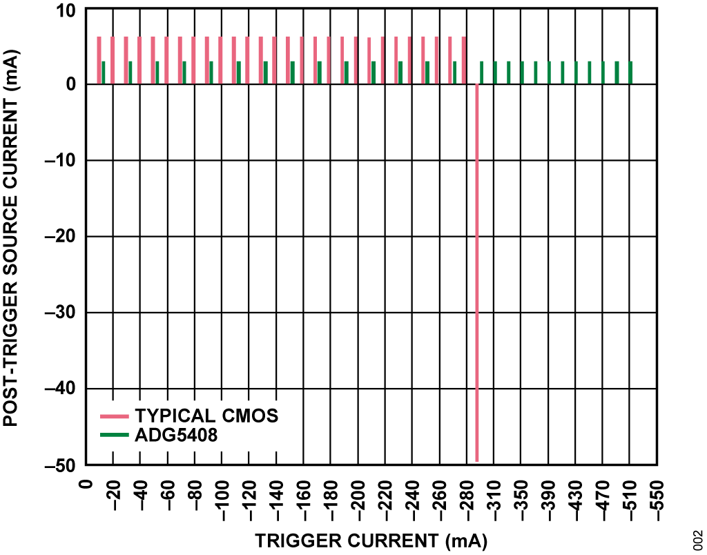
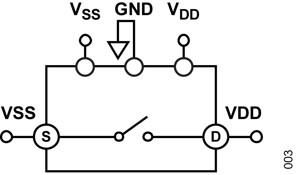
Figure 2 shows the comparison of results between a typical CMOS switch, with epitaxial layer, and the ADG5408 when subjected to a latch-up test. During the test, a stress current is applied to the pin for 1 ms, called the trigger, and the current at the pin is measured after the trigger. This particular test is conducted with the switch set to open, the drain (D) set to VDD, and the source (S) set to VSS, as depicted in Figure 3. The voltage of the source is then driven beyond VSS until the required trigger current is achieved. If latch-up has not occurred, then the current at the pin returns to its pretrigger value. After latch-up has occurred, the pin continues to draw current without being driven by the trigger voltage. This can only be stopped by powering down the part.
From Figure 2, it can be seen that this typical CMOS switch reaches a latch-up current at −290 mA, while the ADG5408 did not latch up until the test ended at −510 mA.