Robust, Fail-Safe Biasing Circuit for AC-Coupled Multidrop LVDS Bus
Abstract
Low-Voltage Differential Signaling (LVDS) has been used widely in high-speed digital-signal interconnections. A popular bus topology connects multiple LVDS receivers to a 100Ω differential twisted pair driven by an LVDS transmitter, which is called the multidrop LVDS bus. The AC-coupling method is often used in the multidrop bus. This application note examines the traditional fail-safe biasing circuit of the multidrop bus and identifies its most common weakness as component variation. The article proposes an alternative robust circuit structure for the fail-safe biasing.
This article was also featured in Engineering Journal, vol. 60 (PDF, 386kB).
LVDS signaling is used widely in high-speed digital-signal interconnections, especially in digital video and camera signals. One of the popular bus topologies, the multidrop LVDS bus, connects multiple LVDS receivers to a 100Ω differential twisted pair driven by an LVDS transmitter. This bus structure is a convenient way to form a multiplex for LVDS signal routing. Additionally, more LVDS interconnections are using AC coupling to avoid ground-level shift and common-mode interference.
Figure 1 shows the block diagram of a typical multidrop LVDS bus. The connection length between the bus and the receiver inputs should be as short as possible. The fail-safe biasing circuit shown in Figure 1 provides a common-mode bias around 1.2V. When the bus is not driven by the Tx, or the bus has no state transition for a long time, the circuit also sets a small, 50mV to 100mV differential voltage to drive the LVDS receiver output to a determined logic state. For a general discussion of LVDS fail-safe circuits, refer to Application Note 3662: Understanding LVDS Fail-Safe Circuits.
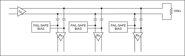
Figure 1. Short connections should be used between the bus and receiver inputs of an AC-coupled, LVDS multidrop bus.
There is a significant difference in the biasing between the multidrop bus and a point-to-point connection: the receivers in a multidrop bus must be high impedance, as compared to the point-to-point connection in which the receiver's input impedance must match the 100Ω impedance of the differential link. The variations of the resistor values are, therefore, a common weakness in the traditional fail-safe biasing circuit. This application note examines that traditional fail-safe circuit design, discusses the problem of component variations, and proposes a new robust biasing circuit.
Traditional Biasing Circuit and Its Weakness
The most common, traditional fail-safe biasing circuit consists of two resistor voltage-dividers at the two LVDS input pins. The implementation is depicted in Figure 2a. The resistor values are chosen so the voltages at both input pins are around 1.2V and the voltage difference of the two input pins is -50mV. The voltages at these two input pins are calculated under the nominal resistor values marked in Figure 2A. When the bus is not driven, this voltage difference will make the receiver output to be logic-low.
If, however, one considers resistor tolerance, the value of the differential voltage can change significantly. Assuming the use of all 1%-tolerant resistors, Figure 2b shows that the voltage difference can reach -90mV, a worst-case negative variation. Alternatively, at the opposite extreme, Figure 2c shows that the voltage difference can be as low as -16mV. Consequently, with a ±1% resistance change, the fail-safe differential input could change from -80% to +68%.
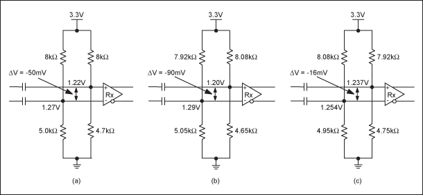
Figure 2. Commonly used fail-safe biasing circuit is shown (a) with nominal resistor values, (b) in a design that produces the greatest voltage differences at ±1% tolerance, and (c) in a design that produces the smallest voltage differences at ±1% tolerance.
A large differential fail-safe voltage is a notable weakness of this traditional circuit design. The large voltage difference causes several reactions: the duty cycle for logic-high or low becomes unbalanced; the triggering threshold moves up at one side of the input and reduces the slow rate at the triggering point, thus causing the receiver's intrinsic jitter to increase. As Figure 2c illustrates, moreover, the low value of the voltage difference might not be enough to activate the fail-safe function.
To overcome the mentioned weaknesses in the traditional biasing circuit, consider the following new biasing circuit that is very robust against resistor variations.
New Fail-Safe Biasing Circuit
A new topology for a fail-safe biasing circuit generates a relatively constant differential voltage regardless of the resistor variation. Figure 3 diagrams the new circuit.
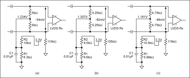
Figure 3. A robust fail-safe biasing circuit is shown (a) with nominal resistor values, (b) in a design that produces the greatest voltage differences at ±5% tolerance, and (c) in a design that produces the smallest voltage differences at ±5% tolerance.
In the new circuit, the common-mode voltage is supplied to the two input pins from a common source. The differential voltage is generated by a pulldown (or pullup) resistor on one input pin. From the values shown in Figure 3, we see that even with ±5% resistors, the fail-safe differential voltage only changes between -15% to +15%, which is far more robust than the circuit shown in Figure 2. This new circuit can be used for LVDS products that have an internal common pullup fail-safe circuit, such as the MAX9169/MAX9170 and MAX9174/MAX9175, or circuits that have a weak internal common-mode biasing, like the MAX9242/MAX9244/MAX9246/MAX9254, MAX9218, and MAX9248 deserializer products.