AN-2016: Using the ADuM4136 Isolated Gate Driver and LT3999 DC-to-DC Converter to Drive a 1200 V SiC Power Module
Introduction
The success of power developments, such as electric vehicles, renewable energies, and energy storage systems depend on the efficient implementation of electrical power conversion schemes. The core of a power electronic converter contains specialized semiconductor devices and the strategy used to switch these semiconductors on and off, which is achieved with gate drivers.
State-of-the-art wideband devices, such as silicon carbide (SiC) and gallium nitride (GaN) semiconductors feature increased capabilities, such as high voltage ratings from 600 V to 2000 V, low channel impedance, and fast switching speeds up to the megahertz range. These capabilities augment the requirements from gate drivers, for example, shorter propagation delays and improved short-circuit protection via desaturation.
This application note demonstrates the advantages of the ADuM4136 gate driver, a single-channel device with an output drive capability of up to 4 A, a maximum common-mode transient immunity (CMTI) of 150 kV/μs, and fast fault management that includes desaturation protection.
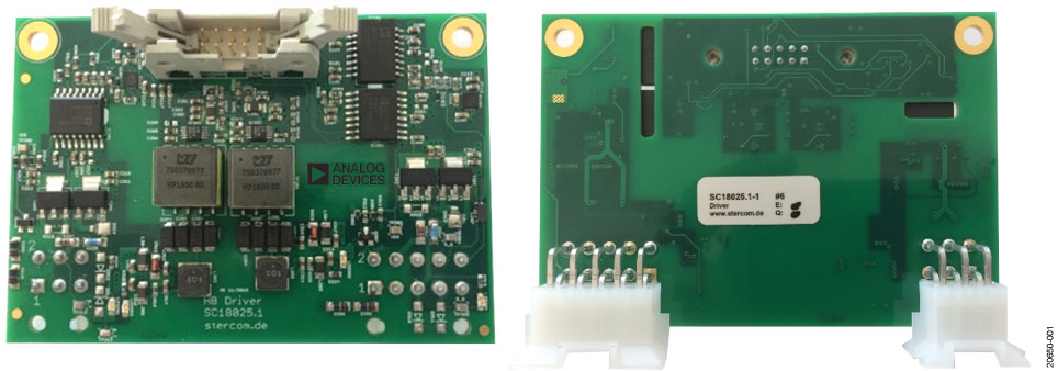
A gate driver unit (GDU) for SiC power devices was developed in collaboration with Stercom Power Solutions GmbH showcases the capabilities of the ADuM4136 (see Figure 1). The board is powered with a bipolar, isolated supply based on a push-pull converter that was built with the LT3999 power driver. This monolithic, high voltage, high frequency, dc-to-dc conversion driver features 1 A dual switches with a programmable current limit, frequency synchronization up to 1 MHz, a wide operating range of 2.7 V to 36 V, and a shutdown current of <1 μA.
The solution was tested on a SiC metal-oxide semiconductor field-effect transistor (MOSFET) power module (F23MR12W1M1_ B11) with a 1200 V drain source breakdown voltage, typical channel resistance of 22.5 mΩ, and pulsed drain current capability of 100 A, with maximum rated gate source voltages of −10 V and +20 V.
This application note evaluates the dead time generated by the solution and investigates the total propagation delay introduced by the GDU. Desaturation detection is tested for protection of the SiC devices from overload and short-circuit conditions.
The fast response of the solution is verified by the results of the tests.

Test Setup
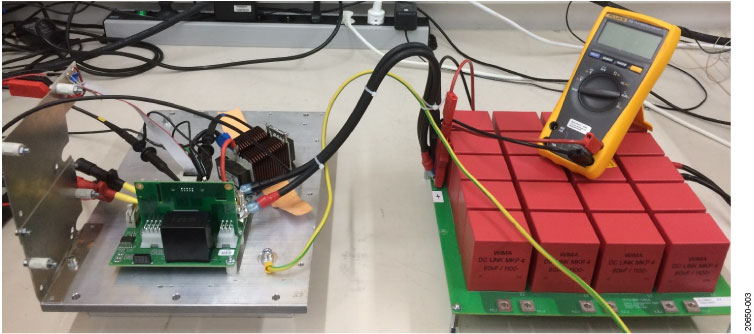
The full setup used for the reported tests is shown in Figure 2. A high voltage, dc input supply (V1) is placed across the power module. A 1.2 mF, decoupling foil capacitor bank (C1) is added across the input. The output stage is a 38 μH inductor (L1) that can be connected to the high-side or low-side of the power module during the desaturation protection test. Table 1 summarizes the test setup power components.


| Components | Value |
| V1 | 0 V to 1000 V |
| C1 | 1.2 mF |
| SiC Power Module (FF23MR12W1M1_B11) | 1200 V, 23 mΩ |
| L1 | 38 μH |
The GDU shown in Figure 4 receives the switching signals from a pulse wave generator. These signals are passed to an integrated dead time generation circuit, implemented with the LT1720 ultra fast, dual-channel comparator, whose output is fed to two ADuM4136 devices. The ADuM4136 gate drivers provide isolated signals to the gate terminals and receive isolated signals from the drain terminals of the two SiC MOSFETs in the power module. The output stages of the gate drivers are supplied with isolated power by a push-pull converter, built with the LT3999 dc-to-dc driver that is fed by an external, 5 V dc power supply. Temperature measurement of the SiC module is implemented with the ADuM4190 high-accuracy isolated amplifier. The ADuM4190 is powered by the LT3080 low dropout (LDO) linear regulator.
Figure 3 shows the experimental setup and Table 2 describes the equipment used in the desaturation protection test.

| Equipment | Manufacturer | Part Number |
| Oscilloscope | Rohde & Schwarz | HMO3004, 500 MHz |
| DC Power Supply | Komerci | QJE3005EIII |
| Gate Driver Unit (GDU) | Stercom | SC18025.1 |
| Pulse Wave Generator | IB Billmann | PMG02A |
| Digital Multimeter (DMM) | FLUKE | Fluke 175 |
| High Voltage Differential Probe | Testec | TT-SI 9010 |
| AC Rogowski Current Probe | PEM | CWT mini |
Test Results
Dead time and Propagation Delay
Hardware dead time is introduced by the GDU to avoid a short circuit in the half-bridge power module, which can occur when the high-side and low-side SiC MOSFETs are turned on or turned off (see Figure 4). Note that the delayed PWM_B signal is indicated within this document as PWM_B_D.


In the propagation delay test, dead time is measured on the signal chain of the bottom driver, which is excited by the (active low) input to the GDU PWM_B signal. The dead time generation is realized using resistor-capacitor (RC) filters with the LT1720 ultra fast comparators. Figure 5 to Figure 8 show the results of the propagation delay test. See Table 3 for descriptions of the signals shown in Figure 5 to Figure 8.
| Symbol | Signal Function | Channel Number |
| VGS_B | MOSFET gating | 2 |
| PWM_B_D | After comparator | 3 |
| PWM_B | Input to GDU | 4 |
When the PWM_B input signal is pulled low, the comparator changes its delayed PWM_B_D output state from high to low and the dead time is determined by the RC circuit (~160 ns, see Figure 5).


When the SiC MOSFETs are turned off and the PWM_B input signal is pulled high, the PWM_B_D delay time is negligible (~20 ns) in comparison to the delay time measured when the SiC MOSFETs are turned on, as shown in Figure 6.


The delay times after the PWM_B_D dead time generation and the VGS_B signals toggle, for both turn on and turn off, are measured as shown in Figure 7 and Figure 8. These short delay times are 66 ns and 68 ns, respectively, and are the delays introduced by the ADuM4136.


The total propagation delay time (dead time plus propagation delay) for turn on is ~226 ns, and for turn off is ~90 ns. Table 4 gives a summary of the results for propagation delay times.
| Event | Toggled Signal, High-Low | Toggled Signal, Low-High | Dead Time (ns) | Driver Delay Time (ns) | Total Propagation Delay Time (ns) |
| Device Turned On | PWM_B, PWM_B_D | Gate Signal | 160 | 66 | 226 |
| Device Turned Off | Gate Signal | PWM_B, PWM_B_D | 22 | 68 | 90 |
Desaturation Protection
Desaturation protection against a high voltage short circuit of the driving switch is integrated onto the ADuM4136 IC.
In this application, each gate driver monitors the voltage from the drain to source terminals (VDS) of its MOSFET indirectly, by checking that the voltage at its DESAT pin (VDESAT) does not exceed the reference desaturation voltage level, VDESAT_REF, which varies between 8.66 V and 9.57 V (VDESAT_REF = 9.2 V typical). Moreover, the value of VDESAT depends on the MOSFET operation and external circuitry: two high-voltage-protection diodes and a Zener diode (see Table 6 and the Schematics section).
The value of VDESAT can be calculated with the following equation:
VDESAT = VZ + 2 × VDIODE_DROP + VDS
where:
VZ is the Zener diode breakdown voltage.
VDIODE_DROP is the forward voltage drop of each protection diode.
During turn off, the DESAT pin is pulled low internally and no saturation event is engaged. Additionally, the MOSFET voltage, (VMOSFET) is high and two diodes are reverse-biased, which protects the DESAT pin.
During turn on, the DESAT pin is released after an internal blanking time of 300 ns, the two protection diodes are forward-biased, and the Zener diode breaks down. Here, whether the VDESAT voltage goes above the VDESAT_REF value depends on the value of VDS.
Under normal operation, the VDS and VDESAT voltages remain low. When a high current passes through the MOSFET, the VDS voltage increases and causes the VDESAT voltage level to rise above VDESAT_REF.
In this event, the ADuM4136 gate driver output pin (VOUT) is driven low during 200 ns and desaturates the MOSFET, and a FAULT signal with a delay of <2 μs is generated for the gate driver signal (VGS) to immediately lock. These signal can only be unlocked by the RESET pin.
The detection voltage level depends on the value of VDS and can be programmed to any level by choosing the appropriate Zener diode with a breakdown voltage, VZ. In turn, the MOSFET current (ID) for desaturation can be estimated based on VDS as described in the MOSFET manufacturer data sheet.
Two desaturation protection tests were performed with gate pulses for both high-side and low-side MOSFETs. Different fault currents were tested in each test by choosing different Zener diodes. The tested current levels are summarized in Table 4, assuming that maximum VDESAT_REF = 9.57 V (maximum), and nominal VDIODE_DROP = 0.6 V.
Low-Side Test
The low-side desaturation protection test was performed by varying the input voltage (V1) from 100 V to 800 V at a room temperature of 25°C (see Figure 9).


Figure 10 to Figure 17 show the results of the low-side desaturation protection test. Table 5 describes the signals shown in Figure 10 to Figure 17.
| Channel Number | Signal Name |
| 1 | FAULT |
| 2 | VDS |
| 3 | ID |
| 4 | VGS |


In Figure 16 and Figure 17, the desaturation protection was triggered for a current of ~125 A at 25°C, and the fault status pin was triggered low after a delay of around 1.34 µs.


Similar tests were run for the high-side of the power module, where the desaturation protection was triggered for a current of ~160 A at 25°C, with the fault status pin triggered low after 1.32 μs.
The results for the low-side and high-side tests show that the desaturation detection with current levels close to the ones programmed can be reported by the gate driving solution at a high speed of <2 μs (see Table 6).
| Test | Zener Breakdown Voltage, VZ (V) | Detection Voltage Level, VDS (V) | Detection Current Level, ID at 25°C (A) | Detection Current Level, ID at 125°C (A) |
| Low-Side | 5.1 | 3.27 | 116 | 95 |
| High-Side | 4.3 | 4.07 | 140 | 110 |
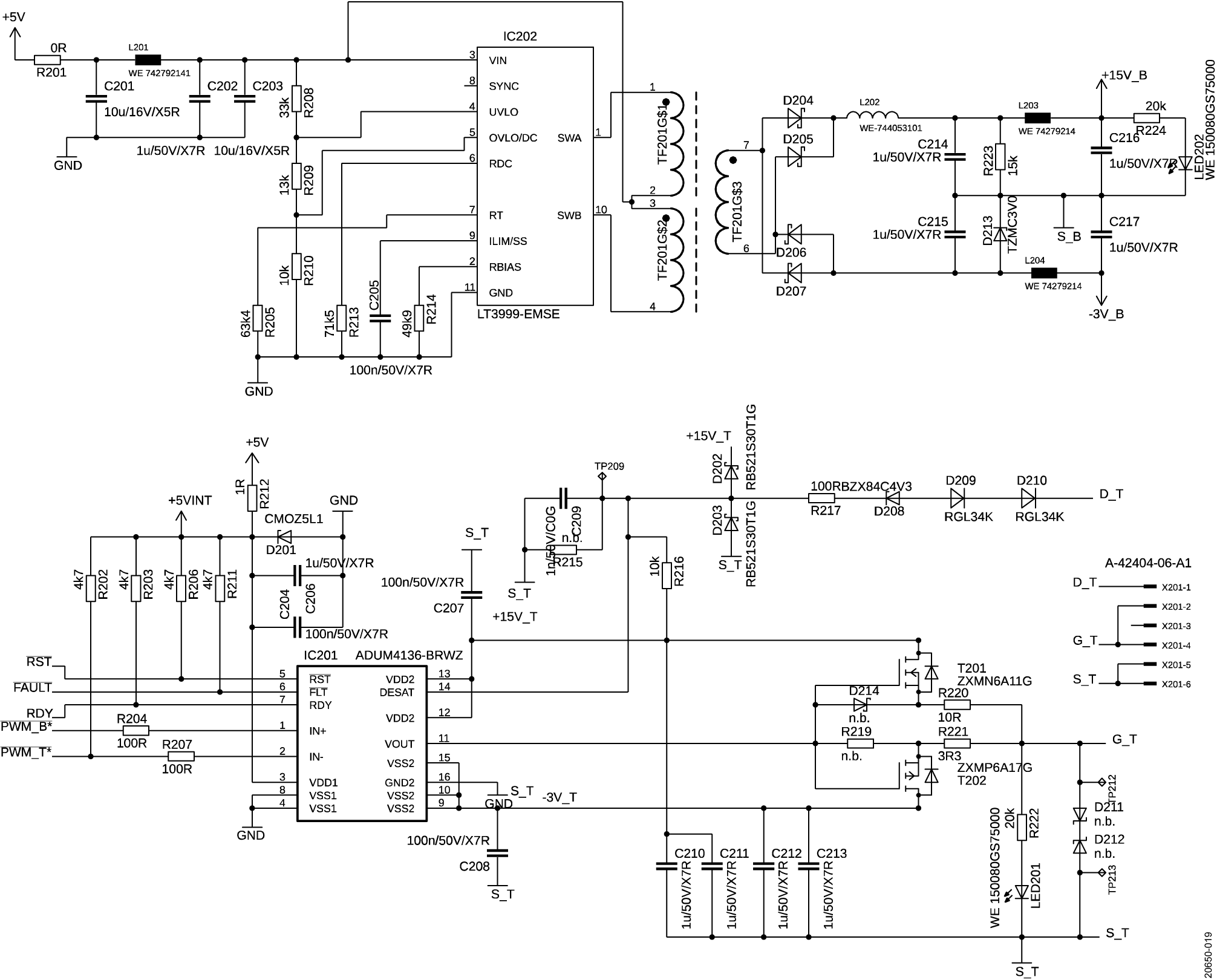
Schematics
Figure 18 to Figure 20 to show the schematics for the ADuM4136 gate driver board.


Conclusion
The ADuM4136 gate driver features short propagation delay and fast overcurrent fault reporting via desaturation protection. These advantages, aligned with adequate external circuitry design, can satisfy the stringent requirements for exploiting the capabilities that state-of-the-art wide-band devices such as SiC and GaN semiconductors can offer.
The test results in this application note provide data from a full gate driving solution for driving a SiC MOSFET module under high voltage, with an ultra fast response, and adequate fault management via desaturation protection. This gate driving solution is powered by a low-noise, compact, power converter built with the LT3999, which provides isolated power of adequate voltage levels with low shutdown currents and soft-start capabilities.
Authors

