AN-1583: High Precision, Low Power, Low Cost Pulse Oximeter Infrared and Red Current Sinks Using the ADA4505-2 10 μA, Zero Input, Crossover Distortion Op Amp, the ADR1581 Precision Shunt Voltage Reference, and the ADG1636 Dual SPDT Switches
Circuit Function and Benefits
Current sources or current sinks are key circuits used broadly in medical, industrial, communication, and other types of equipment for sensor excitation. A good example is the current sources (sinks) needed to drive the internal infrared (IR) LED and red LED in a pulse oximetry sensor.
A pulse oximeter is a noninvasive medical device used for continuously measuring the percentage of hemoglobin (Hb) saturated with oxygen and the pulse rate of a patient. Hemoglobin that is carrying oxygen (oxyhemoglobin) absorbs light in the IR region of the spectrum. Hemoglobin that is not carrying oxygen (deoxyhemoglobin) absorbs visible red light. In pulse oximetry, a clip containing two LEDs (sometimes more, depending on the complexity of the measurement algorithm) and the light sensor (photodiode) is placed on the finger or earlobe of the patient. One LED emits red light (wavelengths of 600 nm to 700 nm), and the other emits light in the near IR (wavelengths 800 nm to 900 nm) region. The clip is connected by a cable to a processor unit. The LEDs are rapidly and sequentially excited by two current sources (one for each LED) whose dc levels depend on the LED being driven, based on manufacturer requirements. The detector is synchronized to capture the light from each LED as the light is transmitted through the tissue.
Low power, precision current sources (if the current flows into the load) or current sinks (if the current flows out of the load) used in pulse oximeter designs are required to deliver a few decades of milliamps (hundreds of milliamps for legacy products).
The active elements in these circuits are a low power precision operational amplifier, a precision shunt voltage reference, and a metal-oxide semiconductor field effect transistor (MOSFET) or a bipolar transistor. To save power, an analog switch can be added to power off the current source and sink when the current source and sink is in standby mode. When an ultraprecision design is required, an ultraprecision series voltage reference can be used instead of the shunt voltage reference.
An excellent low power, low cost precision amplifier to use in this medical application is the 10 µA, zero input, crossover distortion ADA4505-2. A good ultralow power, low cost precision shunt voltage reference to accompany the amplifier is the 1.25 V ADR1581 (A grade). An excellent choice for the analog switch is the 1 Ω, on-resistance ADG1636 dual, single-pole, double throw (SPDT) switch.
The maximum quiescent currents for the devices are as follows when these devices are operated from a power supply rail of 5 V and working under the industrial temperature range of –40°C to +85°C: one-half the ADA4505-2 (15 µA), ADR1581 (70 µA), and ADG1636 (1 µA). These numbers add up to a total of 86 µA current consumption per circuit, which is suitable for portable and battery-powered instruments.
Current sources (sinks) implemented using the ADA4505-2, the ADR1581, and the ADG1636 are characterized by being precise, low power, cost effective, flexible, and small in printed circuit board (PCB) footprint.
Circuit Description
An example design of a dc current sink driving the pulse oximeter red LED and infrared LED is shown in Figure 1. These dc current sinks allow 10.3 mA and 15.2 mA to flow through the red LED and infrared LED, respectively.

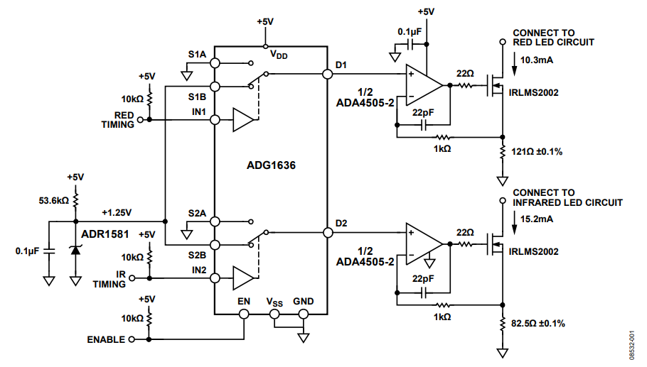
To maximize battery life, the current sinks are turned on only when needed. One-half of the ADG1636 SPDT analog switch is used to connect or disconnect the 1.25 V voltage reference to or from each current circuit.
When the current sinks are driving their respective LEDs, the ADR1581 (A grade) 1.25 V voltage reference is buffered by onehalf the ADA4505-2. The IRLMS2002 N channel MOSFET is connected as a source follower and is inside the op amp feedback loop, which forces the voltage across the current setting resistor (121 Ω or 82.5 Ω) to exactly 1.25 V and in turn sets the current sources to 10.3 mA or 15.2 mA, respectively. In essence, the ADA4505-2 is acting as both a voltage reference buffer and current switch control.
The equation that sets each current sink value is
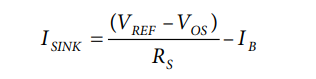
where:
VREF is the 1.25 V voltage reference.
RS is the 121 Ω or 82.5 Ω current sink resistors.
VOS is the offset voltage of the ADA4505-2.
IB is the bias current of the ADA4505-2.
If the VOS and IB of the amplifier are ignored to simplify the circuit analysis, the ISINK is the 10.3 mA or 15.2 mA current through the red LED or infrared LED.
The current sinks are turned off by disconnecting the voltage reference from its current sink resistor and connecting this resistor to ground.
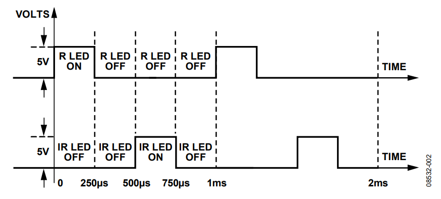
When the current sinks are on, each is on only a certain amount of time, and not at the same time. This time is set by the duty cycle of the waveform driving its corresponding current sink (Pin IN1 and Pin IN2 of the ADG1636 switches). These waveforms are pulses with a duty cycle of approximately 25% and a typical period of 1 ms (1 kHz), which means that each current sink is on during 250 µs in a 1 ms period. A typical timing of these red and infrared current sinks is shown in Figure 2.

Calculate the total current consumption of both current sinks with this timing by the following equation:
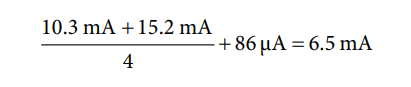
This equation results in a total of less than 6.5 mA out of the 5 V supply needed to obtain a pulse oximetry reading. Note that the 86 µA is the previously calculated current consumption of the ADA4505-2, ADR1581, and ADG1636 combination, and this is only 1.3% of the total 6.5 mA needed. Therefore, these three active elements add a negligible load to the battery.
The VOS error term in the equation not only accounts for the offset voltage of the amplifier, but also for all the errors caused by the nonideal behavior of the op amp. Mathematically account for each of these errors as an additional VOS reflected back to the input of the op amp. By using a precision amplifier like the ADA4505-2, the total sum of all these errors is negligible compared to the inherent offset voltage of the op amp.
The VOS of the ADA4505-2 is 3 mV maximum, which represents an error of 0.24% in the sink current. By the same reasoning, the IB of 2 pA maximum in the ADA4505-2 gives an error that can be considered as zero when compared to the 10.3 mA and 15.2 mA required out of the red current sink and infrared current sink.
If the 0.8% maximum initial accuracy of the ADR1581 and the 0.1% sink resistor tolerance (chosen for this design) are added to this VOS error of 0.24%, the total worst case error is 1.14%, and the uncertainty analysis error is 0.83%. Taking into account the Gaussian distribution curves of the errors from each of the contributing elements (voltage reference, sink resistor, and op amp) in this uncertainty analysis, the less pessimistic expected error is 0.28% (see Holman, J. P., Experimental Methods for Engineers, McGraw-Hill, Fourth Edition, 1984).
The error allowable in the current sink depends on the degree of accuracy needed in the pulse oximeter reading. In a red LED and infrared LED, the accuracy of the current driving the LEDs is directly proportional to the accuracy of the radiant flux (radiant output power) of the LEDs. This radiant flux is a measure of how much power is contained in the light being emitted. Therefore, high LED current accuracy means LED radiant flux high accuracy prediction. A typical radiant flux vs. forward current curve is shown in Figure 3 for the Hamamatsu L5276, L5586, and L6286 infrared LEDs.


Regarding the other elements in the design, the 22 pF capacitors improve stabilization (in-loop compensation) of the ADA4505-2 amplifiers (see Analog Dialogue, “Ask the Applications Engineer—25.” Analog Devices.). The 1 kΩ feedback resistors provide some current limiting into the inverting pin of the amplifiers. The 22 Ω resistors, in series with the ADA4505-2 outputs, serve two purposes. One purpose is to prevent possible oscillation when driving the input capacitance (CISS) of the IRLMS2002 N channel MOSFET. The second purpose is to dampen some of the transient response of the N channel MOSFETs when the MOSFETs turn on and off. These resistors and capacitances may need some further optimization in the specific application.
Table 1 shows the calculated (ideal) and measured values on both red current sink and infrared current sink for the design in Figure 1 at ambient temperature.
| Current Sink | Ideal Value (mA) |
Measured Value (mA) |
Error (%) |
| Red | 10.331 | 10.325 | –0.06 |
| Infrared | 15.152 | 15.168 | +0.11 |
Excellent layout, grounding, and decoupling techniques must be used to achieve the desired performance from the circuits discussed in this note (see Tutorial MT-031 and Tutorial MT-101).
Common Variations
A common variation in this circuit is to replace the voltage reference with a digital-to-analog-converter (DAC). The output of the DAC delivers different voltages depending on the level of light needed out of the red LED and infrared LED. The great benefit of the ADA4505-2 is that, being a zero crossover distortion op amp, its VOS remains constant through the entire input voltage range. The VOS remaining constant avoids the necessity of calibrating the system every time the DAC changes its output to create a different current sink level. One time calibration is therefore sufficient when the ADA4505-2 is working in conjunction with the DAC. Also, the ADG1636 switch can be removed because the DAC can output a 0 V signal to disable the current sink when not needed.
The use of the IRLMS2002 N channel MOSFET allows this design to be used for currents up to hundreds of milliamps (special attention must be placed in ensuring the IRLMS2002 N channel MOSFET safe operating area is not violated). When the current levels are in the order of decades of milliamps, the reliable and cost-effective BSS138 N channel MOSFET can be used instead.
If the accuracy and temperature drift of the total design has stringent requirements, use a more accurate and lower temperature coefficient drift voltage reference, such as the high precision series voltage reference ADR127 or the higher accuracy B grade of the ADR1581. Also, select a tighter tolerance and low temperature drift for the current sink resistor. Choose a very low VOS precision amplifier, for instance the auto-zero (zero drift) AD8629 (2.7 V to 5 V) or the OP07D (8 V to 36 V).
When high precision current sinks are not required, and depending on the total design tolerance requirements, an all purpose, cost-effective op amp can be used. Good examples of these devices are the AD8515 (1.8 V to 5 V), AD8542 (2.7 V to 5.5 V), AD8529 (2.7 V to 12 V), AD8566 (4.5 V to 16 V), and OP275 (9 V to 44 V).
References
Analog Dialogue. “Ask the Applications Engineer—25.” Analog Devices.
AN-968 Application Note, Current Sources: Options and Circuits. Analog Devices.
Holman, J. P., Experimental Methods for Engineers, McGrawHill, Fourth Edition, 1984.
MT-035 Tutorial, Op Amp Inputs, Outputs, Single-Supply, and Rail-to-Rail Issues. Analog Devices.