AN-1361: AD7293 Closed-Loop for Power Amplifier Drain Current Control
Introduction
The AD7293 from Analog Devices, Inc., includes four complete closed-loop power amplifier (PA) drain current controllers on one chip. It offers functionality for monitoring and control of current, voltage, and temperature integrated into a single lead frame chip scale package (LFCSP) solution that is serial port interface (SPI) compatible.
The device features a 4-channel, 12-bit successive approximation register (SAR), analog-to-digital converter (ADC), eight 12-bit digital-to-analog converters (DACs) (four bipolar and four unipolar with configurable output ranges), a ±1.25°C accurate internal temperature sensor, and eight general-purpose input/output (GPIO) pins. The device also includes limit registers for alarm functions and four high-side current sense amplifiers to measure current across external shunt resistors. These amplifiers can be optionally set to operate as part of four independent closed-loop drain current controllers.


Figure 1. Typical High Power Amplifier (HPA) Monitor and Control Application Diagram.
Closed-Loop Current Control
A high accuracy, 2.5 V internal reference is provided to drive the DACs and the ADC. The 12-bit ADC monitors and digitizes an internal temperature sensor, and two inputs for external diode temperature sensors are included.
The bipolar DACs, as well as the four current sensors in the AD7293, can be configured to operate as four independent closed-loop drain current controllers. The bipolar DAC sets the power amplifier (PA) current, and it maintains this constant current. The BI-VOUT2 pin creates a loop with RS2+ and RS2−, for example. Changes in current are seen as a voltage across the current sense resistor, and the current sense amplifier voltage is fed back to the summing amplifier. The current sense amplifier voltage is compared against the DAC voltage and, if there is an error, the integrator resolves the output of the device, adjusting the gate voltage of the external PA until the error in the loop is zero.
Follow the defined power-up sequence in the AD7293 data sheet to ensure the PA is protected during power-up and that registers are used to tune the loop function. This application note is an in depth exploration of the configuration options for the AD7293 closed-loop mode.
The measurement results, simulations, and guidelines are provided to assist radio designers in making decisions about the configuration of the AD7293, as well as making choices about the external circuitry. The HMC1099 gallium nitride (GaN) broadband power amplifier is referenced as the PA.
Closed-Loop Considerations
The AD7293 contains circuitry to implement closed-loop control of the drain current in an RF power amplifier. This circuitry consists of the following:
- A DAC to define the target current, represented as a voltage, VSET, between 0 V and 1.25 V.
- A summing node to calculate the difference between the target current and the actual current.
- An integrator, with programmable time constant, τI.
- A current sense amplifier to measure the voltage, VSENSE, across a sense resistor, RS, located in series with the PA drain.
At the gate of the PA, a network is required to combine the low frequency bias signal generated by the integrator with the high frequency radio frequency (RF) signal. The current control loop is represented by a low-pass filter with time constant as follows:
RGCG = τG
where τG is typically in the range of 5 μs ≤ τG ≤ 50 μs.


Figure 2. Diagram of System.
From Figure 2, the closed-loop transfer function can be determined using the following equation:

where gm is the transconductance of the PA.
To extract the damping ratio, ζ, use the following equation:
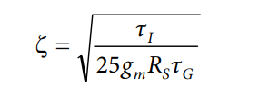
To achieve critical damping (ζ = 1, the fastest possible settling with no overshoot), use the following equation:
τI = 25gmRSτG
If a damping ratio of less than 1 is chosen, use the following equation to predict the overshoot:


Figure 3. Overshoot vs. Damping Ratio for a Second-Order System.
RSENSE Selection
The steady state value of VSENSE is given by the following equation:
VSENSE = (4/25)VSET
Therefore, for the maximum value of VSET, 1.25 V, VSENSE = 0.2 V.
VSENSE sets an upper limit on the value of RS.
RS ≤ 0.2/IDS(MAX)
where IDS(MAX) is the drain current at the maximum required PA gain.
In some cases, it may be desirable to choose a smaller value for RS, for the following benefits:
- Reduced power dissipation in the sense resistor.
- Improved loop dynamics.
- Common sense resistor value for multiple PA types.
- Design margin to guarantee that maximum gain can always be reached.
However, these benefits are at the expense of dynamic range and setpoint resolution.


Figure 4. PA Gain vs. Drain Current (IDS) of HMC1099 PA.
PA Transconductance
The transconductance of the PA varies as a function of drain current. In terms of loop damping, the worst case is when gm is highest. Therefore, after the maximum PA gain required is determined, use the value of gm at this gain to select τI.


Figure 5. PA Transconductance (gm) vs. Drain Current (IDS) of HMC1099 PA.
Worked Example
Using the example of Figure 4, set the gain to a maximum of 18.5 dB. The gate filter network has a time constant, τG, of 30 μs.
IDS (18.5dB) = 0.1 A
Therefore, select RS as follows:
RS = 0.2/0.1 = 2 Ω
Based on Figure 5,
gm (18.5dB) = 0.8 S
This equation gives a target value for τI as follows:
τI = 25gmRSτG
τI = 25 × 0.8 × 2 × 30 μs
τI = 1.2 ms
Table 1 shows the settings available in the AD7293.
| Code | Integrator Time Constant (τI) | Calculated Damping Ratio for This Example | Overshoot (%) |
| 1 | 2.352 ms | 1.4 | 0.0 |
| 2 | 1.218 ms | 1.01 | 0.0 |
| 3 (default) | 840 μs | 0.84 | 0.77 |
| 4 | 650 μs | 0.74 | 3.15 |
| 5 | 538 μs | 0.67 | 5.87 |
| 6 | 462 μs | 0.62 | 8.35 |
| 7 | 408 μs | 0.58 | 10.68 |
The default setting for τI of Code 3 (840 μs) results in an overshoot of 0.77% for a step change in setpoint, which is typically acceptable. If no overshoot is required, implement any of the following actions:
- Reduce RS to 1.4 Ω (reduced dynamic range, setpoint resolution).
- Choose τI of Code 2 for slower settling (see Table 1).
- Change the gate filter to give τG = 21 μs (increased noise from control loop).
Adding a Third Pole
It may be useful to add a filter at the input to the current sense amplifier to reject high frequency disturbances (see Figure 6).


Figure 6. Current Control Loop with Additional Filter at Current Sense Input.
The resulting transfer function is:

For an existing two-pole system with ζ = 1, set τS ≤ (1/10)τG to avoid affecting the loop response.
Use a computer simulation to predict the effect of adding a third pole.
Based on the values chosen in the Worked Example section, Figure 7 shows a transient simulation of the effect of the sense filter, for a step change of VSET from 0 V to 1 V.


Figure 7. Overshoot Introduced by Third Pole at Current Sense Input.
Closed-Loop Update Rate
The preceding analysis in the Worked Example section assumes that all the components in the loop operate in continuous time. In the AD7293, the current sense amplifier and integrator sample their inputs with a period of 16.8 μs. This sampling results in the voltage at the integrator output consisting of discrete steps, which can be observed as a tone of frequency, 1/16.8 μs ≈ 60 kHz, during VSENSE transitions. This tone can be reduced in amplitude by the gate filter, so that it does not affect the PA output.
The sampling introduces a criterion for loop stability, even with only two poles in the loop.
τI/gmRS > 52.5 μs
where:
τI = 840 μs.
gm = 0.8.
RS = 2 Ω.
Therefore, τI/gmRS = 840/0.8 × 2 = 525 μs.
Power Amplifier Gate Current Considerations
The gate current of the power amplifier is a function of the drive level. Typically, the gate current increases close to compression if the radio is running at 6 dB from compression. In normal operation, gate currents of greater than 2 mA are not expected in either direction for output powers less than 1 dB compression point (P1dB) minus 6. The AD7293 can comfortably supply this level of current.
The AD7293 can source current, but it is important to note that the gate current changes as a function of the compression level, and this must be kept in mind when characterizing the radio.
Power dissipation must be considered at high current levels, such as 20 mA × 5 V × 4 channels = 400 mW. The AD7293 package has a θJA of 27°C/W.
The bipolar DAC output channels are capable of providing a significant amount of current to the gate of the power amplifier while also maintaining linearity performance, as shown in Figure 8, when the power amplifier is running close to compression. However, take care to ensure the system functions as expected.


Figure 8. Bipolar DAC Integral Nonlinearity (INL), RS = 500Ω to AVDD, 0 Ω, and 500 Ω to AGND.
Clamping and Protection
A protection circuit is implemented that clamps the bipolar DAC voltage outputs to −5 V (AVSS) when the 5 V supply fails. Typically, the trip point is between 3.5 V and 4 V. This clamp switch has a 500 Ω to 600 Ω resistance associated with it. Consider this resistance when examining the PA drain current considerations.


Figure 9. Bipolar DAC Output on Removing AVDD.
On the AD7293, the bipolar DAC outputs are clamped to −3 × VCLAMPx during power-up. This clamp ensures that when the AD7293 controls a depletion mode device, the PA is not turned on to full power when the AD7293 is powered up. Figure 10 shows the typical settling time for the bipolar DAC output to clamp. Figure 11 shows the typical settling time for the bipolar DAC output to wake up from clamping.


Figure 10. Closed Loop to Clamp Settling Time, VCLAMPx = 1.5 V.


Figure 11. Wake Up from Clamp Settling Time, VCLAMPx = 1.5 V.
Power-Up Sequencing
See the AD7293 data sheet for instructions on which registers to write to during power-up to protect the PA.
Authors

