HMC8205
RECOMMENDED FOR NEW DESIGNS0.3 or 0.4 GHz to 6 GHz, 35 W, GaN Power Amplifier
- Part Models
- 3
- 1ku List Price
- price unavailable
Part Details
HMC8205BF10 Features
- High PSAT: 46 dBm
- High power gain: 20 dB
- High PAE: 38%
- Instantaneous bandwidth: 0.3 GHz to 6 GHz
- Supply voltage: VDD = 50 V at 1300 mA
- 10-lead LDCC package
HMC8205BCHIPS Features
- High output power: 45.5 dBm typical at PIN = 24 dBm
- High power gain: 22 dB typical at PIN = 24 dBm
- High PAE: 40% typical at PIN = 28 dBm
- Die size: 4.8 mm × 3.4 mm × 0.1 mm
The HMC8205BF10 is a gallium nitride (GaN) broadband power amplifier delivering 45.5 dBm (35 W) with 38% power added efficiency (PAE) across an instantaneous bandwidth of 0.3 GHz to 6 GHz. No external matching is required to achieve full band operation. Additionally, no external inductor is required to bias the amplifier. Also, dc blocking capacitors for the RFIN and RFOUT pins are integrated into the HMC8205BF10.
The HMC8205BF10 is ideal for pulsed or continuous wave (CW) applications, such as military jammers, wireless infrastructure, radar, and general-purpose amplification.
The HMC8205BF10 amplifier is a 10-lead ceramic leaded chip carrier (LDCC).
The HMC8205BCHIPS is a gallium nitride (GaN), broadband power amplifier that delivers 45.5 dBm (35 W) with 40% power added efficiency (PAE) across an instantaneous bandwidth of 0.4 GHz to 6 GHz. No external matching is required to achieve full band operation. No external inductor is required to bias the amplifier. In addition, dc blocking capacitors for the RFIN and RFOUT pins are integrated into the HMC8205BCHIPS.
The HMC8205BCHIPS is ideal for pulsed or continuous wave (CW) applications, such as military jammers, wireless infrastructure, radar, and general-purpose amplification.
APPLICATIONS
- Military jammers
- Commercial and military radar
- Power amplifier stage for wireless infrastructure
- Test and measurement equipment
Documentation
Data Sheet 2
Application Note 2
Video 1
Product Selection Guide 1
Analog Dialogue 1
Webcast 2
ADI has always placed the highest emphasis on delivering products that meet the maximum levels of quality and reliability. We achieve this by incorporating quality and reliability checks in every scope of product and process design, and in the manufacturing process as well. "Zero defects" for shipped products is always our goal. View our quality and reliability program and certifications for more information.
| Part Model | Pin/Package Drawing | Documentation | CAD Symbols, Footprints, and 3D Models |
|---|---|---|---|
| HMC8205BCHIPS | CHIPS OR DIE | ||
| HMC8205BF10 | 10 ld LDCC (11.43x17.32mm) | ||
| HMC8205BF10-50 | 10 ld LDCC (11.43x17.32mm) |
| Part Models | Product Lifecycle | PCN |
|---|---|---|
|
Dec 12, 2017 - 17_0199 Change in First Level Packaging for HMC1086F10, HMC1087F10, HMC8205BF10. |
||
| HMC8205BF10 | PRODUCTION | |
This is the most up-to-date revision of the Data Sheet.
Software Resources
Can't find the software or driver you need?
Request a Driver/SoftwareTools & Simulations
ADIsimRF
ADIsimRF is an easy-to-use RF signal chain calculator. Cascaded gain, noise, distortion and power consumption can be calculated, plotted and exported for signal chains with up to 50 stages. ADIsimRF also includes an extensive data base of device models for ADI’s RF and mixed signal components.
Open ToolS-Parameter 2
Sys-Parameter Models for Keysight Genesys
Sys-Parameter models contain behavioral parameters, such as P1dB, IP3, gain, noise figure and return loss, which describe nonlinear and linear characteristics of a device.
Open ToolEvaluation Kits


HMC8205 Evaluation Board
Resources


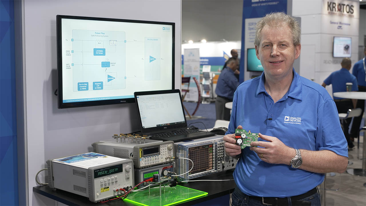
Pulser Plus Reference Design for GaN PA Biasing and Sequencing