AD9528
RECOMMENDED FOR NEW DESIGNSJESD204B/JESD204C Clock Generator with 14 LVDS/HSTL Outputs
- Part Models
- 2
- 1ku List Price
- Starting From $10.59
Part Details
- 14 outputs configurable for HSTL or LVDS
- Maximum output frequency
- 6 outputs up to 1.25 GHz
- 8 outputs up to 1 GHz
- Dependent on the voltage controlled crystal oscillator (VCXO) frequency accuracy (start-up frequency accuracy: <±100 ppm)
- Dedicated 8-bit dividers on each output
- Coarse delay: 63 steps at 1/2 the period of the RF VCO divider output frequency with no jitter impact
- Fine delay: 15 steps of 31 ps resolution
- Typical output to output skew: 20 ps
- Duty cycle correction for odd divider settings
- Output 12 and Output 13, VCXO output at power-up
- Absolute output jitter: <160 fs at 122.88 MHz, 12 kHz to 20 MHz integration range
- Digital frequency lock detect
- SPI- and I2C-compatible serial control port
- Dual PLL architecture
- PLL1
- Provides reference input clock cleanup with external VCXO
- Phase detector rate up to 110 MHz
- Redundant reference inputs
- Automatic and manual reference switchover modes
- Revertive and nonrevertive switching
- Loss of reference detection with holdover mode
- Low noise LVDS/HSTL outputs from VCXO used for radio frequency/intermediate frequency (RF/IF) synthesizers
- PLL2
- Phase detector rate of up to 275 MHz
- Integrated low noise VCO
- PLL1
The AD9528 is a two-stage PLL with an integrated JESD204B/JESD204C SYSREF generator for multiple device synchronization. The first stage phase-locked loop (PLL) (PLL1) provides input reference conditioning by reducing the jitter present on a system clock. The second stage PLL (PLL2) provides high frequency clocks that achieve low integrated jitter as well as low broadband noise from the clock output drivers. The external VCXO provides the low noise reference required by PLL2 to achieve the restrictive phase noise and jitter requirements necessary to achieve acceptable performance. The on-chip VCO tunes from 3.450 GHz to 4.025 GHz. The integrated SYSREF generator outputs single shot, N-shot, or continuous signals synchronous to the PLL1 and PLL2 outputs to time align multiple devices.
The AD9528 generates six outputs (Output 0 to Output 3, Output 12, and Output 13) with a maximum frequency of 1.25 GHz, and eight outputs with a maximum frequency of up to 1 GHz. Each output can be configured to output directly from PLL1, PLL2, or the internal SYSREF generator. Each of the 14 output channels contains a divider with coarse digital phase adjustment and an analog fine phase delay block that allows complete flexibility in timing alignment across all 14 outputs. The AD9528 can also be used as a dual input flexible buffer to distribute 14 device clock and/or SYSREF signals. At power-up, the AD9528 sends the VCXO signal directly to Output 12 and Output 13 to serve as the power-up ready clocks.
Applications
- High performance wireless transceivers
- LTE and multicarrier GSM base stations
- Wireless and broadband infrastructure
- Medical instrumentation
- Clocking high speed ADCs, DACs, DDSs, DDCs, DUCs, MxFEs; supports JESD204B/JESD204C
- Low jitter, low phase noise clock distribution
- ATE and high performance instrumentation
Documentation
Data Sheet 1
User Guide 1
Application Note 1
Technical Articles 2
Informational 1
Video 1

Device Drivers 2
Analog Dialogue 1
Webcast 1
ADI has always placed the highest emphasis on delivering products that meet the maximum levels of quality and reliability. We achieve this by incorporating quality and reliability checks in every scope of product and process design, and in the manufacturing process as well. "Zero defects" for shipped products is always our goal. View our quality and reliability program and certifications for more information.
| Part Model | Pin/Package Drawing | Documentation | CAD Symbols, Footprints, and 3D Models |
|---|---|---|---|
| AD9528BCPZ | 72-Lead LFCSP (10mm x 10mm w/ EP) | ||
| AD9528BCPZ-REEL7 | 72-Lead LFCSP (10mm x 10mm w/ EP) |
| Part Models | Product Lifecycle | PCN |
|---|---|---|
|
Jun 26, 2023 - 23_0025 Package Outline Drawing and Data Sheet Revision for Select LFCSP Products in Amkor |
||
| AD9528BCPZ | PRODUCTION | |
| AD9528BCPZ-REEL7 | PRODUCTION | |
|
Jan 29, 2015 - 15_0011 AD9528 specification table 15 changes |
||
| AD9528BCPZ | PRODUCTION | |
| AD9528BCPZ-REEL7 | PRODUCTION | |
This is the most up-to-date revision of the Data Sheet.
Software Resources
Device Drivers 2
Evaluation Software 2
Tools & Simulations
ADIsimCLK Design and Evaluation Software
ADIsimCLK is the design tool developed specifically for Analog Devices' range of ultra-low jitter clock distribution and clock generation products. Whether your application is in wireless infrastructure, instrumentation, networking, broadband, ATE or other areas demanding predictable clock performance, ADIsimCLK will enable you to rapidly develop, evaluate and optimize your design.
Open ToolIBIS Model 1
Evaluation Kits


ADRV9026 and ADRV9029 Evaluation Board
Resources
Software


High speed data acquisition FMC board
Resources
Software


ADRV9008/ADRV9009 Evaluation Board
Resources
Software
AD9528 Evaluation Board
Resources
Software


ADA4961 & AD9680 Analog Signal Chain Evaluation and AD9528 Converter Synchronization
Resources
Software


AD9375 Small Cell Radio Reference Design
Resources
Software


ADRV9375-N/PCBZ and ADRV9371-W/PCBZ Evaluation Board
Resources
Software


ADRV9371-N/PCBZ and ADRV9371-W/PCBZ Boards
Features and Benefits
- Complete Radio Card platform containing AD9371 with:
- 2 x Transmit outputs
- 2 x Receive inputs
- 2 x Observation inputs
- 1x Sniffer path
- Narrow tuning range and Wide tuning range options
- ADRV9371-N/PCBZ matched for 1.8GHz – 2.6GHz
- ADRV9371-W/PCBZ matched for 300MHz – 6GHz
- Complete with high efficiency power supply solution and clocking solution for AD9371
- FMC connector to Xilinx ZC706 motherboard (EK-Z7-ZC706-G).
- Powered from single FMC connector
- Includes schematics, layout, BOM, HDL, drivers and application software
Product Details
The ADRV9371-N/PCBZ and ADRV9371-WPCBZ are radio cards designed to showcase the AD9371, a high performance wideband integrated RF transceiver intended for use in RF applications such as 4G base station, test and measurement applications and software defined radios. The radio cards provide hardware engineers, software engineers and system architects with a single 2x2 transceiver platform for device evaluation and rapid prototyping of radio solutions. All peripherals necessary for the radio card to operate including a high efficiency switcher only power supply solution, and a high performance clocking solution are populated on the board.
Both narrow tuning range and wide tuning range options exist.
The ADRV9371-N/PCBZ is optimized for performance over a narrow tuning range1.8GHz – 2.6GHz. It will exhibit diminished RF performance on tuned RF frequencies outside of this band. This board is primarily intended to provide RF engineers with the ability to connect the AD9371 to an RF test bench (Vector Signal Analyzer, Signal Generator, etc.) and achieve its optimum performance.


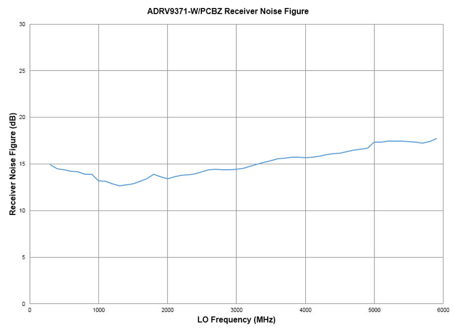
The ADRV9371-W/PCBZ operates over a wide tuning range 300MHz – 6GHz, however the RF performance is tempered by the very wide band front end match. This board is primarily intended for system investigation and bringing up various waveforms from a software team before custom hardware is complete. The objective being for designers to see waveforms, but not being concerned about the last 1dB or 1% EVM of performance.

The board interfaces to the Xilinx ZC706 motherboard (EK-Z7-ZC706-G) (ordered separately).