HMC7044B

RECOMMENDED FOR NEW DESIGNS

High Performance, 3.2 GHz, 14-Output Jitter Attenuator with JESD204B and JESD204C Support

Part Models
2
1ku List Price
Starting From $15.69
Viewing:

Part Details

  • Ultra-low rms jitter: 44 fs typical (12 kHz to 20 MHz) at 2457.6 MHz
  • Noise floor: −156 dBc/Hz at 2457.6 MHz
  • Low phase noise: −141.7 dBc/Hz at 800 kHz, 983.04 MHz output
  • Up to 14 LVDS, LVPECL, or CML type device clocks (DCLKs) from PLL2
  • Maximum CLKOUTx/CLKOUTx and SCLKOUTx/SCLKOUTx frequency up to 3200 MHz
  • JESD204B- and JESD204C-compatible system reference (SYSREF) pulses
  • Narrow-band, dual core VCOs
  • 25 ps analog, and ½ VCO cycle digital delay independently programmable on each of 14 clock output channels
  • SPI-programmable phase noise vs. power consumption
  • SYSREF valid interrupt to simplify JESD204B and JESD204C synchronization
  • Up to 2 buffered voltage-controlled crystal oscillator (VCXO) outputs
  • Up to 4 input clocks in LVDS, LVPECL, CMOS, and CML modes
  • Frequency holdover mode to maintain output frequency
  • Loss of signal (LOS) detection and hitless reference switching
  • 4× GPIOs alarms/status indicators to determine the health of the system
  • External VCO input to support up to 6000 MHz
  • On-board regulators for excellent PSRR
  • 68-lead, 10 mm × 10 mm LFCSP package
HMC7044B
High Performance, 3.2 GHz, 14-Output Jitter Attenuator with JESD204B and JESD204C Support
HMC7044B Functional Block Diagram HMC7044B Pin Configuration
Add to myAnalog

Add product to the Products section of myAnalog (to receive notifications), to an existing project or to a new project.

Create New Project
Ask a Question

Documentation

Learn More
Add to myAnalog

Add product to the Products section of myAnalog (to receive notifications), to an existing project or to a new project.

Create New Project

Software Resources


Hardware Ecosystem

Parts Product Life Cycle Description
Clock Distribution Devices 2
LTC6955 LAST TIME BUY Ultralow Jitter, 7.5GHz, 11 Output Fanout Buffer Family
HMC7043 RECOMMENDED FOR NEW DESIGNS

High Performance, 3.2 GHz, 14-Output Fanout Buffer with JESD204B/JESD204C

Modal heading
Add to myAnalog

Add product to the Products section of myAnalog (to receive notifications), to an existing project or to a new project.

Create New Project

Tools & Simulations

IBIS Model 1

ADIsimCLK

Open Tool

Evaluation Kits

eval board
QUAD-MxFE Platform

16Tx/16Rx Direct L/S/C-Band Sampled Phased-Array/RADAR/EW/SATCOM Development Platform

Features and Benefits

Quad-MxFE Digitizing Card
  • Multi-Channel, Wideband System Development Platform Using MxFE
  • Mates With Xilinx VCU118 Evaluation Board (Not Included)
  • 16x RF Receive (Rx) Channels (32x Digital Rx Channels)
    • Total 16x 1.5GSPS to 4GSPS ADC
    • 48x Digital Down Converters (DDCs), Each Including Complex Numerically-Controlled Oscillators (NCOs)
    • 16x Programmable Finite Impulse Response Filters (pFIRs)
  • 16x RF Transmit (Tx) Channels (32x Digital Tx Channels)
    • Total 16x 3GSPS to 12GSPS DAC
    • 48x Digital Up Converters (DUCs) , Each Including Complex Numerically-Controlled Oscillators (NCOs)
  • Flexible Rx & Tx RF Front-Ends
    • Rx: Filtering, Amplification, Digital Step Attenuation for Gain Control
    • Tx: Filtering, Amplification
  • On-Board Power Regulation from Single 12V Power Adapter (Included)
  • Flexible Clock Distribution
    • On-Board Clock Distribution from Single External 500MHz Reference
    • Support for External Converter Clock per MxFE
16Tx / 16Rx Calibration Board
  • Mates to Quad-MxFE Digitizing Card & VCU118 PMOD Interface (Cable Included)
  • Provides Both Individual Adjacent Channel Loopback and Combined Channel Loopback Options
  • Combined Tx Channels Out Via SMA Option
  • Combined Rx Channels In Via SMA Option
  • On-Board Log Power Detectors With AD5592R Output To VCU118 Over PMOD
  • On-Board Power Regulation from Single 12V Power Adapter (Included)
Software Features and Benefits
Easy Control Tools and Platform Interfaces to Simplify Software Framework Developments:
  • IIO Oscilloscope GUI
  • MATLAB Add-Ons & Example Scripts
  • Example HDL Builds including JESD204b/JESD204c Bring-Up
  • Embedded Software Solutions for Linux and Device Drivers
  • MATLAB System Applications GUI
Software Reference Design Examples for ADEF Applications to Reduce Prototyping Time:
  • Multi-Chip Synchronization for Power-Up Phase Determinism
  • System-Level Amplitude/Phase Alignment Using NCOs
  • Low-Latency ADC-to-DAC Loopback Bypassing JESD Interface
  • pFIR Control for Broadband Channel-to-Channel Amplitude/Phase Alignment
  • Fast-Frequency Hopping
  • Calibration Board MATLAB Driver File
  • FPGA Programming MATLAB Script

Product Details

The Quad-MxFE System Development Platform contains four MxFE software defined, direct RF sampling transceivers, as well as associated RF front-ends, clocking, and power circuitry. The target application is phased array radars, electronic warfare, and ground-based SATCOM, specifically a 16 transmit/16 receive channel direct sampling phased array at L/S/C band (0.1 GHz to ~5GHz). The Rx & Tx RF front-end has drop-in configurations that allow for customized frequency ranges, depending on the user’s application.

The Quad-MxFE System Development Platform highlights a complete system solution. It is intended as a testbed for demonstrating multi-chip synchronization as well as the implementation of system level calibrations, beamforming algorithms, and other signal processing algorithms. The system is designed to mate with a VCU118 Evaluation Board from Xilinx®, which features the Virtex® UltraScale+ XCVU9P FPGA, with provided reference software, HDL code, and MATLAB system-level interfacing.

In addition to the Quad-MxFE Digitizing Card, the kit also contains a 16Tx / 16Rx Calibration Board that is used to develop system-level calibration algorithms, or otherwise more easily demonstrate power-up phase determinism in situations pertinent to their own use case. The Calibration Board also allows the user to demonstrate combined-channel dynamic range, spurious, and phase noise improvements and can also be controlled via a free MATLAB add-on when connected to the PMOD interface of the VCU118.

The system can be used to enable quick time-to-market development programs for applications like:

  • ADEF (Phased-Array, RADAR, EW, SATCOM)
  • Communications Infrastructure (Multiband 5G and mmWave 5G)
  • Electronic Test and Measurement

eval board
AD-SYNCHRONA14-EBZ

Multichannel System Clocking Device

Features and Benefits

Processing System

  • Raspberry Pi 4, ARM Cortex-A72, 2GB SDRAM

User Interfaces

  • Gigabit Ethernet
  • 2 × USB 3.0 ports
  • 2 × USB 2.0 ports
  • SPI interface
  • GPIO
  • 2 bicolor LEDs
  • Male pin header

Clock Processing Devices

  • HMC7044 (High Performance, 3.2 GHz, 14-Output Jitter Attenuator)
  • AD9545 (1 PPS Synchronizer and Adaptive Clock Translator)

Clock Outputs

  • 4 x TWINAX LVPECL AC&DC coupled, 100Ω diff
  • 2 x SMA LVPECL AC coupled*
  • 4 x SMA CMOS*
  • 4 x SMA LVDS AC coupled*

*Configurable differential outputs, 50Ω diff

Clock Inputs

  • 3 differential 100Ω SMA clock inputs
  • PPS input
  • SYNC input
  • 10MHz input

Internal references

  • 100Mhz and 122.88Mhz Ultra-Low Phase Noise VCXO's (-165dBc/Hz)
  • 40Mhz and 38.4Mhz TCXO's (±1ppm) 50MHz OCXO(+/- 10ppb)
  • Internal references are software configurable

Power supply

  • DC 12V, 3A barrel jack

Product Details

The AD-SYNCHRONA14-EBZ is an ideal self-contained device to use in evaluation and prototyping of applications that need a highly accurate frequency and phase-controlled source clock. It is designed around the Analog Devices AD9545 and HMC7044 and greatly simplifies clock distribution and multi-channel synchronization in complex systems. It is intended to be used by trained professionals in a laboratory environment, and not intended as an end product for commercial use. It can be taken as a complete reference design and customised as required for any end customer applications. Full design details are made available free of charge.

The AD-SYNCHRONA14-EBZ comes in a 1U mechanical form factor. Using popular industry connector SMA and TwinAX interfaces most labs will already have the needed cables.

With its internal OCXO it can operate in standalone mode or be fed from a choice of external sources, such as 3 separate high speed differential clock inputs, a 10MHz reference and 1PPS. This flexibility combined with the capability to select either of the internal VCXO options of 100MHz or 122.88MHz, gives almost unlimited choice for the frequency of interest and accuracy needed for a wide variety of application areas. 

APPLICATIONS

  • High accuracy reference clock distribution
  • Systems clocked from a single source
  • Clocks derived from 100MHz or 122.88MHz
  • Phased Array Systems, RADAR, EW, SATCOMS, SDR
  • Bench Equipment
  • Remote controlled operation

eval board
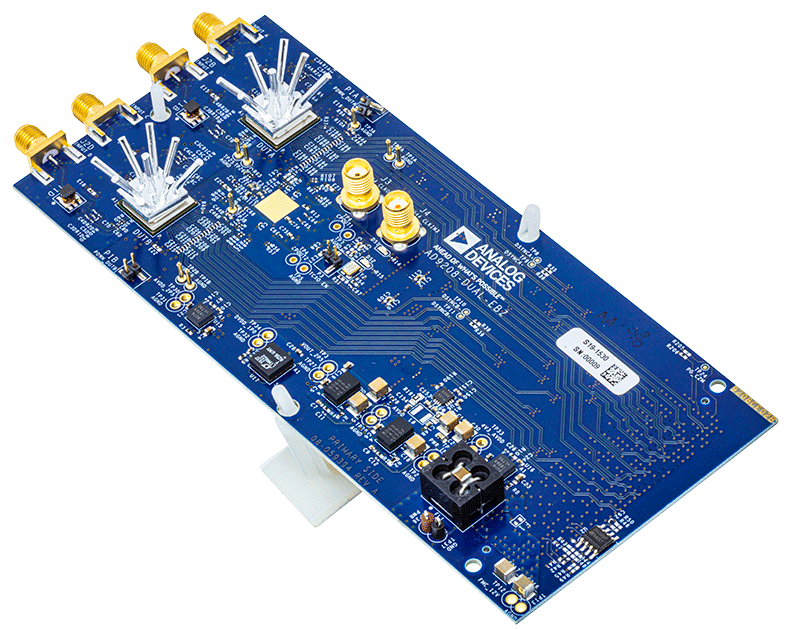
EVAL-AD9208

Single AD9208 and Dual AD9208 Evaluation Boards

Features and Benefits

Two evaluation options are available: AD9208-3000EBZ and AD9208-DUAL-EBZ.

  • AD9208-3000 Features
    • Full featured evaluation board for the AD9208-3000. 
    • Wide band Balun driven input. 
    • No external supply needed. Uses 12V-1A and 3.3V-3A supplies from FMC connector. 
    • Single software interface for device control and analysis through ACE. 
  • AD9208-DUAL Features
    • Demonstration board showing multi-chip synchronization of two AD9208 ADCs using HMC7044.
    • Self contained clocking for the ADCs as well as the FPGA.
    • Single external 12V supply.
    • Interfaces with VCU118 or similar FPGA development board with FMC+ (Vita57.4) connector.
    • Uses Analog Devices’ JESD204B IP framework.
    • Low SWaP high efficiency power delivery using Silent Switcher technology.
    • Full software support available Analog Devices Wiki Page.

Product Details

The AD9208-3000EBZ supports the AD9208-3000, a 14-bit, 3GSPS dual analog-to-digital converter (ADC). The device has an on-chip buffer and a sample-and-hold circuit designed for low power, small size, and ease of use. This device is designed support direct RF sampling analog signals of up to 5 GHz. The 3 dB bandwidth of the ADC input is greater than 9 GHz. The AD9208 is optimized for wide input bandwidth, high sampling rate, excellent linearity, and low power in a small package.

This reference design provides all of the support circuitry required to operate the ADC in its various modes and configurations. It is designed to interface directly with the ADS7-V2EBZ data capture card, allowing users to download captured data for analysis. The device control and subsequent data analyses can now be done using the ACE software package.

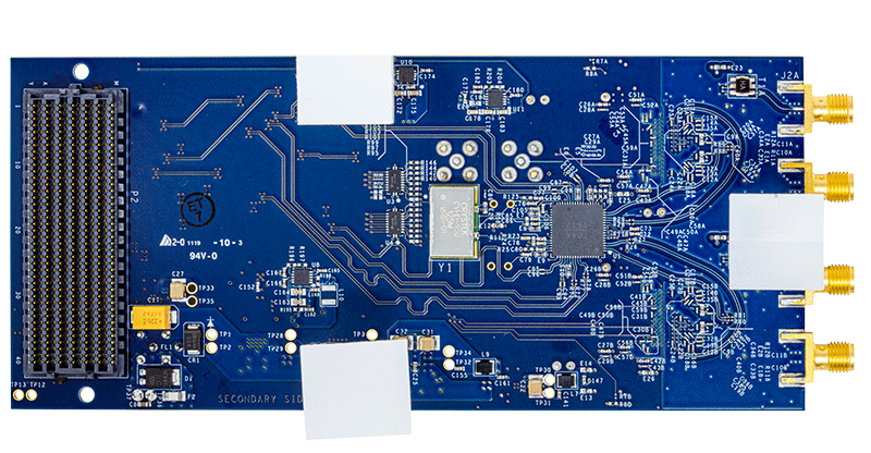
The AD9208-DUAL-EBZ is a demonstration board designed to show multi-chip synchronization using JESD204B subclass1 protocol. The AD9208-3000 is a 14-bit, 3GSPS dual analog-to-digital converter (ADC). This device is designed support direct RF sampling analog signals of up to 5 GHz. The 3 dB bandwidth of the ADC input is greater than 9 GHz. The AD9208 is optimized for wide input bandwidth, high sampling rate, excellent linearity, and low power in a small package. The HMC7044 is a high performance, dual-loop, integer-N jitter attenuator capable of performing reference selection and generation of ultralow phase noise frequencies for high speed data converters with either parallel or serial (JESD204B type) interfaces. The LTM8074 is a 40VIN, 1.2A continuous, 1.75A peak, step-down µModule® (power module) regulator. The Silent Switcher architecture minimizes EMI while delivering high efficiency at frequencies up to 2.2MHz.

This reference design provides all of the support circuitry required to operate the ADC in its various modes and configurations. It is designed to easily demonstrate multi-chip synchronization using the JESD204B subclass1 protocol. The board is designed to interface directly with FPGA development boards with FMC+ (Vita57.4) connector.

eval board
EVAL-HMC7044

HMC7044 Evaluation Kit

Features and Benefits

  • Simple power connection using USB connection and on-board LDO voltage regulators
  • LDOs can be bypassed for power measurements
  • AC-coupled differential SMA connectors
  • SMA connectors for
    2 reference Inputs
    6 clock outputs
    1 VCXO output
  • Microsoft Windows®–based evaluation software with simple graphical user interface
  • On-board PLL loop filter
  • Easy access to digital input/output and diagnostic signals via input/output header (4 GPIOs)
  • Status LEDs for diagnostic signals
  • USB computer interface

Product Details

The HMC7044 meets the requirements of multi-carrier GSM and LTE base-station designs and offers a wide range of clock management and distribution features to simplify baseband and radio card clock tree designs. The high performance dual-loop core of the HMC7044 enables the base station designer to attenuate the incoming jitter of a primary system reference clock, such as a CPRI source, with the help of the narrow-band configured first PLL loop, which disciplines an external VCXO, and generate the low phase noise, high frequency clocks with the wider-band second PLL to drive data converter sample clock inputs.


The EK1HMC7044LP10B evaluation board is a compact, easy-to-use platform for evaluating all the features of the HMC7044. A 122.88 MHz VCXO is mounted on the evaluation board to provide a complete solution. All inputs and outputs are configured as differential on the evaluation board.


Full specifications on the HMC7044 are available in the product data sheet, which should be consulted in conjunction with this user guide when working with the evaluation board.

QUAD-MxFE Platform
16Tx/16Rx Direct L/S/C-Band Sampled Phased-Array/RADAR/EW/SATCOM Development Platform
ADQUADMXFE1EBZ Board ADQUADMXFE1EBZ Evaluation Board - Top View ADQUADMXFE1EBZ Evaluation Board - Bottom View Quad-MxFE Evaluation Board with Lights QUAD-MxFE Block Diagram ADQUADMXFE-CAL Board ADQUADMXFE-CAL Evaluation Board - Top View ADQUADMXFE-CAL Evaluation Board - Bottom View
AD-SYNCHRONA14-EBZ
Multichannel System Clocking Device
AD-SYNCHRONA14-EBZ Evaluation Board - Front View AD-SYNCHRONA14-EBZ Evaluation Board Evaluation Board - Back View AD-SYNCHRONA14-EBZ Evaluation Board
EVAL-AD9208
Single AD9208 and Dual AD9208 Evaluation Boards
AD9208-3000 Evaluation Board AD9208-3000 Evaluation Board - Top View AD9208-3000 Evaluation Board - Bottom View AD9208-DUAL Evaluation Board AD9208-DUAL Evaluation Board - Top View AD9208-DUAL Evaluation Board - Bottom View
EVAL-HMC7044
HMC7044 Evaluation Kit
EK1HMC7044LP10B

Latest Discussions

Recently Viewed