Synchronizing Sample Clocks of a Data Converter Array
The requirements of higher system bandwidth and resolution in a variety of applications from communications infrastructure to instrumentation drive up the demand for connecting multiple data converters in an array form. Designers must find low noise and high accuracy solutions to clock and synchronize a large array of data converters using the common JESD204B serial data converter interface.
Clock generation devices containing jitter attenuation functions, internal VCOs, and a multitude of outputs and many synchronization management functions, are now coming to market to address this system problem. In many real-life applications, however, the sheer number of required clocks in a data converter array exceeds what may be feasible to obtain from a single IC component. Designers often resort to connecting multiple clock generation and clock distribution components together, thus, creating a broad clock tree.
This article provides a real-life case study of how to build a flexible and reprogrammable clock expansion network that maintains not only an excellent phase noise/jitter performance, but also passes on the required synchronization information from the first device of the clock tree to the last one with deterministic control.
Introduction
The evolution of wireless communications systems from 3G to 4G and LTE (and 5G, currently under specification discussions) have been critical technology drivers for high speed data conversion and synchronization. There is a confluence of factors that push up the required data bandwidths in cellular base stations. The primary factors are the growth in the number of subscribers, demand for richer multimedia content, and new applications in machine-to-machine communications using the global cellular infrastructure. As a consequence, designers are looking at new and innovative RF transceiver architectures with higher channel counts using techniques such as active antenna designs, massive MIMO, and advanced beamforming. Systems with large numbers of inputs and outputs make use of multiple transmission paths and require large counts of ADC and DAC components. Given the scale of data conversion requirements, sample clock generation and synchronization become significant design challenges. In complex systems, the number of clock signals required can easily increase from just a few to hundreds, as can be seen in Figure 1.

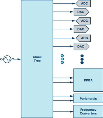
Figure 1. Data converter system with a clock tree.
JESD204B standard defines a serial data interface, which is used to reduce the number of data inputs/outputs between wideband data converters and other system ICs. This reduction of data I/O quantity addresses the problem of interconnecting high speed, high bit count data converters. The ability to offer wideband data converters with fewer interconnects simplifies the PCB layout and allows smaller form factor realization without impacting overall system performance. These improvements are important to address the system size and cost constraints of most of the applications, including wireless infrastructure, portable instrumentation, military applications, and medical ultrasound equipment.
System Level Considerations
In complex systems with large data converter arrays, the increasing volume of data to be processed requires high SNR (signal-to-noise-ratio) links from antenna to processing units. From a clocking perspective, the SNR is limited by the phase noise of the sampling clock. Poor phase noise performance may degrade the system performance by creating jitter and increasing EVM (error vector magnitude), and thus, severely decreasing SNR. In general, clock signal quality is specified in jitter, which is defined as the integration of phase noise over a set bandwidth of interest. Typically, phase noise integration limits are 10s of kHz to 10s of MHz. However, broadband noise is also critical because high clock signal noise floors will also affect the SNR of the system. A poor sampling clock may also have spurious signal content, which will degrade the SFDR (spurious-free dynamic range). And finally, sampling clock quality should not only be defined in the frequency domain, but also in time domain, when considering parameters such as duty cycle and rise/fall time.
These are the basic system requirements for a sampling clock. However, in large data converter arrays and when synchronization is required between the clocks for different arrays, interchannel skew becomes the critical requirement. The performance in such systems relies on synchronized data arrays and, therefore, is sensitive to the skew between different data converters.
Power consumption is another consideration. Higher power consumption decreases system efficiency, increases temperature and cooling costs, and leads, potentially, to higher failure rates. From a commercial standpoint, the part count and the board space are also important and should be controlled.
Clock Tree Structure
As mentioned, quite often in large scale systems, a single clock IC may not have enough outputs to drive all branches. Clock tree topology may overcome this problem and be able to synchronize multiple parts, devices, or multiple systems. A clock tree topology block diagram is given in Figure 2. Note that each level in the tree introduces a delay component, which is made up of fixed and undetermined portions.

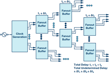
Figure 2. Clock tree block diagram.
These delays may be affected by external factors like voltage and temperature changes, and device-specific process variations. The inaccuracies add up, resulting in potentially intolerable timing variations in ADCs and DACs, which are required to be clocked simultaneously at high frequencies. The high frequencies of operation needed in today’s systems dictate stringent setup and hold times. Although fixed delays can be compensated for with additional effort, undetermined delays cannot be compensated for within the system. A designer’s objective, then, is to minimize or eliminate the undetermined delay element by controlling it in some manner.
In addition to these constraints, the tree structure should be flexible in order to be able to increase the number of branches and control them easily depending on system needs.
A common goal in aligning clocks and minimizing channel skews is to do this function deterministically—that is, repetitively for all devices, and for all power-up sequences. In a JESD204B system, the alignment of local multiframe clocks (LMFCs) is needed to achieve deterministic latency. The interface calls for the reset and alignment of LMFCs at transmitting and receiving devices, using subclass 1 (SYSREF) or subclass 2 (SYNC) definitions. Undetermined delays across the system make the alignment of LMFCs harder to achieve within 1 LFMC period. Consequently, previously mentioned clock tree structures with high accuracy alignment would help the system designers to fulfill the alignment of LMFCs.
Additionally, designers need to ensure that acceptable setup and hold times are observed for SYSREF signals relative to the device clock at each data converter input. If the design uses a single clocking chip, meeting setup and hold times is a straightforward process of ensuring proper timing margins are accounted for, whereas, in multiple-device clock tree structures that are based on simple clock buffers, controlling setup and hold times are more challenging. The proposed clock tree structure with deterministic sync across different layers helps with meeting the setup/hold timing requirements for all SYSREF/device clocks pairs among all layers. This clock tree structure may meet synchronization constraints and phase align the high speed device clocks at every data converter across different layers.
Design of a Clock Tree
A four-level clock tree example is shown in Figure 3, where one main clock generation part (HMC7044) and three-level fanout buffers (HMC7043) are used to create multiple synchronized clocks for sampling boards.

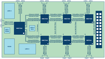
Figure 3. Four-level clock tree example.
One HMC7044 is used as the root of the clock tree; it is a 14-output clock generator with jitter attenuation supporting JESD204B synchronization. HMC7043 devices—14-output fanout buffers—are used at each level of the branches. These parts are fully compatible and their programming feature is very similar, which makes it very easy to match the parts and to increase or decrease the level of clock distribution, adding flexibility to system.
Synchronization may be accomplished between each output at each level of clock tree. In this system, outputs of the HMC7044 can be phase-aligned by SPI commands or more accurately by using a SYNC pulse. The command will reset the common SYSREF timer of the HMC7044, which controls the output dividers for all clocks. All output clock dividers are aligned by the commands from the SYSREF timer simultaneously. The delay from the SYNC command to the SYSREF timer and delay between turn-on and turn-off time is well defined, which provides synchronization with deterministic delay between outputs. Additionally, any output can be programmed to generate a defined number of pulses to be used as SYSREF pulses in the system.
The clock distribution part, HMC7043, also includes a very similar SYSREF timer structure. The device utilizes an RFSYNC signal for alignment. An RFSYNC pulse will start the same process as the SYNC signal of HMC7044, and all outputs will be synchronized with high accuracy. Again the outputs can be set to pulse mode to be used as SYSREF pulses.
The proposed clock tree structure basically uses the SYSREF signals as the RFSYNC signal to the HMC7043 for the next level and maintains phase alignment at the outputs at each level. By careful architecture design, all of these timing signals are deterministic, providing tight skew control. In addition, each part includes an analog delay structure so that any skew difference between outputs, or any line length inequalities, can be compensated at the source.
For complex data converter arrays used in RF systems, different frequencies may be required since ADCs, DACs, FPGAs, local oscillators, and mixers can be clocked at different frequencies. Both the HMC7044 and HMC7043 have built-in dividers that enable generation of multiple frequencies. In addition, the HMC7044 has a dual PLL structure with an integrated VCO that enables generation of a high frequency clock without additional components.
An additional complexity in common communication systems is that most RF front-end units rely on serial interfaces to the transmission/receive blocks, which require that data and clock be embedded/de-embedded by a digital processor or FPGA. This process often produces unwanted reference clock jitter and requires that the jitter attenuation capability is included in large RF clock generation and distribution devices, such as the HMC7044.
The compact solution that can be used in data converter arrays is shown in Figure 4.

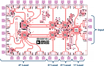
Figure 4. Compact solution of the four-level clock tree.
Test Results
In Figure 5 the skew between all outputs is shown. The yellow and cyan line signals are pulsed SYSREF and continuous clock signals for the 4th level output, which are synchronized without additional delay adjustments. The blue line signal is the continuous SYSREF signal from the HMC7044, and by using the analog delay feature, it is synchronized with the 4th level output. In this example, a total skew of less than 16 ps is obtained.

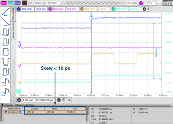
Figure 5. Time domain response of four-level output.
The phase noise performance of the four-level clock tree can be seen in Figure 6. The phase noise of the clock generator is also shown with the lighter blue line. There is no degradation up to 2 MHz offset in the total phase noise. Given the additive noise (additive jitter) of each level, a degradation in the noise floor is inevitable, and may be observed in the graph with the 6 dB increase in the noise in this section. The HMC7044 and HMC7043 have the same output noise floor (about –154 dBc/Hz) and the noise from all four parts degrades to –148 dBc/Hz, which is still an acceptable level for most systems.

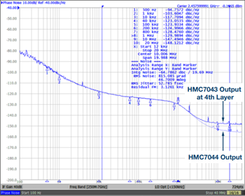
Figure 6. Frequency domain response of four-level output.
The integrated noise from 12 kHz to 20 MHz at 2457.6 MHz calculates to 52.7 fs of jitter rms, only a few fs rms degradation with respect to the output of the HMC7044. In almost all practical systems, this degradation is tolerable, however, if it is not tolerable, the final stage may be substituted with an HMC7044 instead of the HMC7043, which attenuates any accumulated jitter in the clock tree itself.
As mentioned, in systems where a large number of data converters are used, power consumption becomes one of the most critical issues. A critical factor in the power consumption of such a clock tree is the type of signaling used. The output signaling modes of the HMC7044 and HMC7043 may be changed by software control independent from each other, which gives the option of trade-off between power consumption and drive strength vs. frequency. A general guideline is that at low frequencies LVDS may be used with low power consumption whereas at high frequencies LVPECL and CML offer the best performance.
Conclusion
The discussion in this article is applicable across many different systems that utilize distributed, large data converter arrays from wireless infrastructure to military radars to test and measurement systems. Higher frequency and higher bandwidth modulation schemes proposed in the recent 5G communication systems build on the current trends for multiple RF input/output interfaces, which necessitate an increased number of data conversion paths. Additionally, in some of the recent 5G architecture proposals, phased-array antennas are widely discussed as a means to save power and increase the output capacity.
Widely deployed in military communication systems, phased-array techniques not only require a large number of clocks but also require precise synchronization of these clocks.
Another important use case for large data converter arrays are test and measurement systems, where a high volume of data needs to be captured with high sample rates, contributing as little noise as possible, and be processed simultaneously. These systems also require a large number of synchronized clocks. Similarly, with advanced medical imaging systems, data processing throughputs are high and require synchronous operation of parallel data acquisition paths.
As demonstrated here, IC companies are coming up with creative and practical solutions to implement these advanced designs. Components such as the HMC7044 and HMC7043 are developed with system challenges in mind and are aimed at building high performance and flexible clock trees, while maintaining deterministic phase accuracy across multiple levels of clock expansion.
About the Authors
Related to this Article
Industry Solutions
Product Categories
Latest Media 21


