HMC7044
RECOMMENDED FOR NEW DESIGNSHigh Performance, 3.2 GHz, 14-Output Jitter Attenuator with JESD204B and JESD204C Support
- Part Models
- 2
- 1ku List Price
- price unavailable
Part Details
- Ultralow rms jitter: 44 fs typical (12 kHz to 20 MHz) at 2457.6 MHz
- Noise floor: −156 dBc/Hz at 2457.6 MHz
- Low phase noise: −141.7 dBc/Hz at 800 kHz, 983.04 MHz output
- Up to 14 LVDS, LVPECL, or CML type device clocks (DCLKs) from PLL2
- Maximum CLKOUTx/CLKOUTx and SCLKOUTx/SCLKOUTx frequency up to 3200 MHz
- JESD204B-compatible system reference (SYSREF) pulses
- 25 ps analog, and ½ VCO cycle digital delay independently programmable on each of 14 clock output channels
- SPI-programmable phase noise vs. power consumption
- SYSREF valid interrupt to simplify JESD204B synchronization
- Narrow-band, dual core VCOs
- Up to 2 buffered voltage controlled oscillator (VCXO) outputs
- Up to 4 input clocks in LVDS, LVPECL, CMOS, and CML modes
- Frequency holdover mode to maintain output frequency
- Loss of signal (LOS) detection and hitless reference switching
- 4× GPIOs alarms/status indicators to determine the health of the system
- External VCO input to support up to 6000 MHz
- On-board regulators for excellent PSRR
- 68-lead, 10 mm × 10 mm LFCSP package
The HMC7044 is a high performance, dual-loop, integer-N jitter attenuator capable of performing reference selection and generation of ultralow phase noise frequencies for high speed data converters with either parallel or serial (JESD204B type) interfaces. The HMC7044 features two integer mode PLLs and overlapping on-chip VCOs that are SPI-selectable with wide tuning ranges around 2.5 GHz and 3 GHz, respectively. The device is designed to meet the requirements of GSM and LTE base station designs, and offers a wide range of clock management and distribution features to simplify baseband and radio card clock tree designs. The HMC7044 provides 14 low noise and configurable outputs to offer flexibility in interfacing with many different components including data converters, field-programmable gate arrays (FPGAs), and mixer local oscillators (LOs).
The DCLK and SYSREF clock outputs of the HMC7044 can be configured to support signaling standards, such as CML, LVDS, LVPECL, and LVCMOS, and different bias settings to offset varying board insertion losses.
Applications
- JESD204B clock generation
- Cellular infrastructure (multicarrier GSM, LTE, W-CDMA)
- Data converter clocking
- Microwave baseband cards
- Phase array reference distribution
Documentation
Data Sheet 1
User Guide 1
Technical Articles 2
Video 2


Product Selection Guide 1
Device Drivers 1
Analog Dialogue 3
Thought Leadership Page 1
Webcast 3
ADI has always placed the highest emphasis on delivering products that meet the maximum levels of quality and reliability. We achieve this by incorporating quality and reliability checks in every scope of product and process design, and in the manufacturing process as well. "Zero defects" for shipped products is always our goal. View our quality and reliability program and certifications for more information.
| Part Model | Pin/Package Drawing | Documentation | CAD Symbols, Footprints, and 3D Models |
|---|---|---|---|
| HMC7044LP10BE | 68-Lead QFN (10mm x 10mm w/ EP) | ||
| HMC7044LP10BETR | 68-Lead QFN (10mm x 10mm w/ EP) |
| Part Models | Product Lifecycle | PCN |
|---|---|---|
|
Aug 2, 2021 - 21_0135 HMC7044 Data Sheet Revision. |
||
| HMC7044LP10BE | PRODUCTION | |
| HMC7044LP10BETR | PRODUCTION | |
This is the most up-to-date revision of the Data Sheet.
Software Resources
Device Drivers 1
Evaluation Software 0
Can't find the software or driver you need?
Hardware Ecosystem
| Parts | Product Life Cycle | Description |
|---|---|---|
| Clock Distribution Devices 2 | ||
| LTC6955 | LAST TIME BUY | Ultralow Jitter, 7.5GHz, 11 Output Fanout Buffer Family |
| HMC7043 | RECOMMENDED FOR NEW DESIGNS |
High Performance, 3.2 GHz, 14-Output Fanout Buffer with JESD204B/JESD204C |
| Parts | Product Life Cycle | Description |
|---|---|---|
| HMC7044B | High Performance, 3.2 GHz, 14-Output Jitter Attenuator with JESD204B and JESD204C Support |
Tools & Simulations
ADIsimCLK Design and Evaluation Software
ADIsimCLK is the design tool developed specifically for Analog Devices' range of ultra-low jitter clock distribution and clock generation products. Whether your application is in wireless infrastructure, instrumentation, networking, broadband, ATE or other areas demanding predictable clock performance, ADIsimCLK will enable you to rapidly develop, evaluate and optimize your design.
Open ToolIBIS Model 1
Evaluation Kits


16Tx/16Rx Direct L/S/C-Band Sampled Phased-Array/RADAR/EW/SATCOM Development Platform
Resources
Software


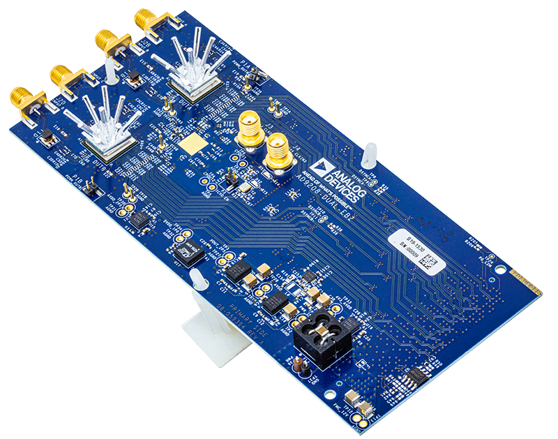

Single AD9208 and Dual AD9208 Evaluation Boards
Resources

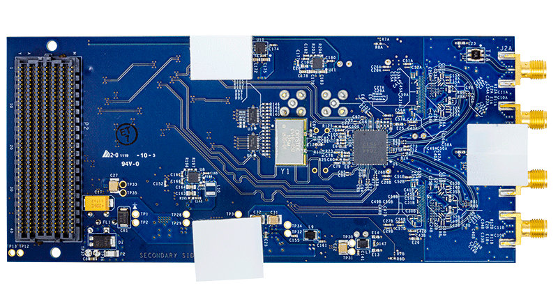
HMC7044 Evaluation Kit
Resources


Multichannel System Clocking Device