HMC1099LP5DE
Obsolete10 Watt GaN Power Amplifier, 0.01 - 1.1 GHz
- Part Models
- 2
- 1ku List Price
- price unavailable
Part Details
- High saturated output power (PSAT): 40.5 dBm typical
- High small signal gain: 18.5 dB typical
- High power added efficiency (PAE): 69% typical
- Instantaneous bandwidth: 0.01 GHz to 1.1 GHz
- Supply voltage: VDD = 28 V at 100 mA
- Internal prematching
- Simple and compact external tuning for optimal performance
- 32-lead, 5 mm × 5 mm, LFCSP package: 25 mm2
The HMC1099LP5DE is a gallium nitride (GaN), broadband power amplifier delivering >10 W with up to 69% PAE across an instantaneous bandwidth of 0.01 GHz to 1.1 GHz, and with a ±0.5 dB typical gain flatness.
The HMC1099LP5DE is ideal for pulsed or continuous wave (CW) applications, such as wireless infrastructure, radars, public mobile radios, and general-purpose amplification.
The HMC1099LP5DE amplifier is externally tuned using low cost, surface-mount components and is available in a compact LFCSP package.
Multifunction pin names may be referenced by their relevant function only.
Applications
- Extended battery operation for public mobile radios
- Power amplifier stage for wireless infrastructures
- Test and measurement equipment
- Commercial and military radars
- General-purpose transmitter amplification
Documentation
Data Sheet 1
Application Note 4
Technical Articles 1
Video 2

Product Selection Guide 1
Webcast 2
ADI has always placed the highest emphasis on delivering products that meet the maximum levels of quality and reliability. We achieve this by incorporating quality and reliability checks in every scope of product and process design, and in the manufacturing process as well. "Zero defects" for shipped products is always our goal. View our quality and reliability program and certifications for more information.
| Part Model | Pin/Package Drawing | Documentation | CAD Symbols, Footprints, and 3D Models |
|---|---|---|---|
| HMC1099LP5DE | 32-Lead LFCSP_CAV (5mm x 5mm w/ EP) | ||
| HMC1099LP5DETR | 32-Lead LFCSP_CAV (5mm x 5mm w/ EP) |
| Part Models | Product Lifecycle | PCN |
|---|---|---|
|
Oct 30, 2018 - 18_0034 Discontinuance of Model Numbers: HMC1132LP5DE, HMC943ALP5DE, HMC1114LP5DE, HMC8500LP5DE and HMC1099LP5DE |
||
| HMC1099LP5DE | Obsolete | |
| HMC1099LP5DETR | Obsolete | |
This is the most up-to-date revision of the Data Sheet.
Software Resources
Can't find the software or driver you need?
Request a Driver/SoftwareHardware Ecosystem
| Parts | Product Life Cycle | Description |
|---|---|---|
| HMC1099PM5E | 10 W (40 dBm), 0.01 GHz to 1.1 GHz, GaN Power Amplifier |
Tools & Simulations
S-Parameter 1
Sys-Parameter Models for Keysight Genesys
Sys-Parameter models contain behavioral parameters, such as P1dB, IP3, gain, noise figure and return loss, which describe nonlinear and linear characteristics of a device.
Open ToolADIsimRF
ADIsimRF is an easy-to-use RF signal chain calculator. Cascaded gain, noise, distortion and power consumption can be calculated, plotted and exported for signal chains with up to 50 stages. ADIsimRF also includes an extensive data base of device models for ADI’s RF and mixed signal components.
Open ToolEvaluation Kits


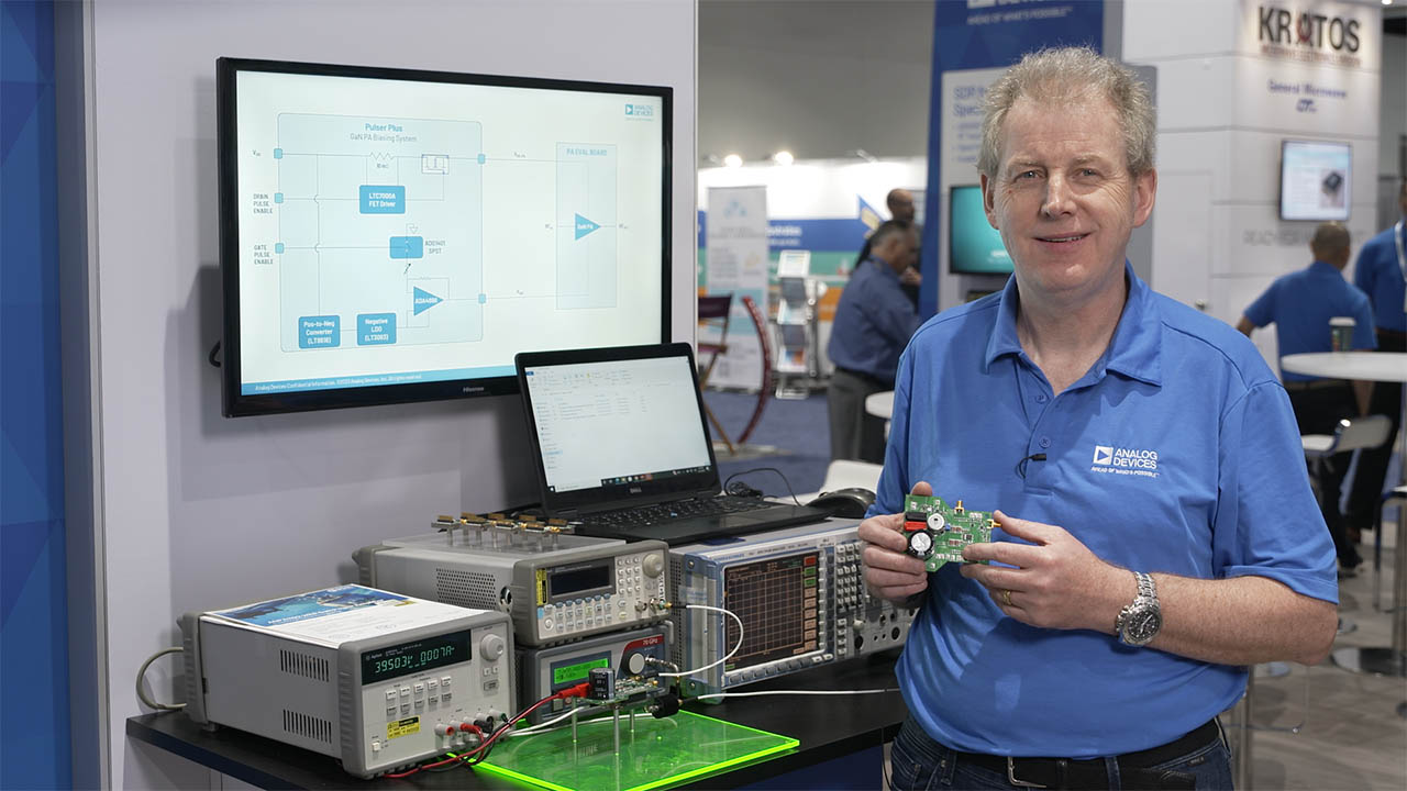
Pulser Plus Reference Design for GaN PA Biasing and Sequencing
Resources

HMC1099 Evaluation Board