ADRF5549
RECOMMENDED FOR NEW DESIGNSReceiver Front End, Dual-Channel, 1.8 GHz to 2.8 GHz
- Part Models
- 3
- 1ku List Price
- Starting From $13.43
Part Details
- Integrated dual-channel RF front end
- 2-stage LNA and high power SPDT switch
- On-chip bias and matching
- Single-supply operation
- Gain
- High gain mode: 35 dB typical at 2.3 GHz
- Low gain mode: 17 dB typical at 2.3 GHz
- Low noise figure
- High gain mode: 1.4 dB typical at 2.3 GHz
- Low gain mode: 1.4 dB typical at 2.3 GHz
- High isolation
- Between RxOUT-ChA and RxOUT-ChB: 50 dB typical
- Between TERM-ChA and TERM-ChB: 62 dB typical
- Low insertion loss: 0.6 dB typical at 2.3 GHz
- High power handling at TCASE = 105°C
- Full lifetime
- LTE average power (9 dB PAR): 40 dBm
- Single event (<10 sec operation)
- LTE average power (9 dB PAR): 43 dBm
- Full lifetime
- High OIP3: 32 dBm typical
- Power-down mode and low gain mode for LNA
- Low supply current
- High gain mode: 85 mA typical at 5V
- Low gain mode: 35 mA typical at 5 V
- Power-down mode: 12 mA typical at 5 V
- Positive logic control
- 6 mm × 6 mm, 40-lead LFCSP
The ADRF5549 is a dual-channel, integrated, RF front-end multichip module designed for time division duplexing (TDD) applications that operates from 1.8 GHz to 2.8 GHz. The ADRF5549 is configured in dual channels with a cascading, two-stage, low noise amplifier (LNA) and a high power, silicon single-pole, double-throw (SPDT) switch.
In high gain mode, the cascaded two-stage LNA and switch offer a low noise figure of 1.4 dB and a high gain of 35 dB with an output third-order intercept point (OIP3) of 32 dBm typical.
In low gain mode, one stage of the two-stage LNA is in bypass mode providing 17 dB of gain at a lower current of 35 mA. In power-down mode, the LNAs are turned off, and the device draws 12 mA.
In transmit operation, when RF inputs are connected to a termination pin (TERM-ChA or TERM-ChB), the switch provides a low insertion loss of 0.6 dB and handles a long-term evolution (LTE) full lifetime average (9 dB peak to average ratio (PAR)) of 40 dBm and 43 dBm for a 9 dB PAR LTE single event (<10 sec) average. The device comes in a RoHS-compliant, compact, 6 mm × 6 mm, 40-lead, lead frame chip-scale package (LFCSP).
Applications
- Wireless Infrastructure
- TDD massive multiple input and multiple output (MIMO) and active antenna systems
- TDD-based communication systems
Documentation
Data Sheet 1
User Guide 1
Design Note 1
Video 2


Product Selection Guide 1
ADI has always placed the highest emphasis on delivering products that meet the maximum levels of quality and reliability. We achieve this by incorporating quality and reliability checks in every scope of product and process design, and in the manufacturing process as well. "Zero defects" for shipped products is always our goal. View our quality and reliability program and certifications for more information.
| Part Model | Pin/Package Drawing | Documentation | CAD Symbols, Footprints, and 3D Models |
|---|---|---|---|
| ADRF5549BCPZN | 40-Lead LFCSP (6mm x 6mm w/ EP) | ||
| ADRF5549BCPZN-R7 | 40-Lead LFCSP (6mm x 6mm w/ EP) | ||
| ADRF5549BCPZN-RL | 40-Lead LFCSP (6mm x 6mm w/ EP) |
This is the most up-to-date revision of the Data Sheet.
Tools & Simulations
S-Parameter 1
Evaluation Kits
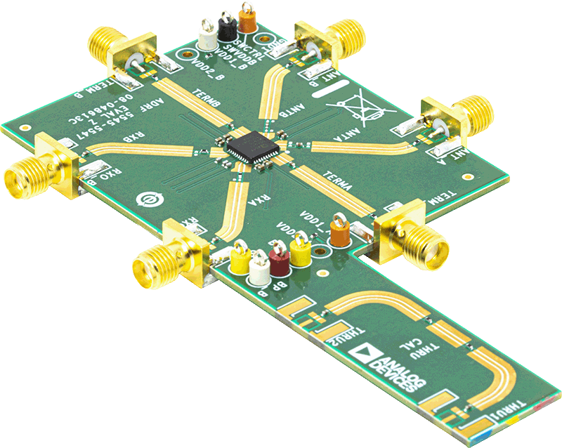


ADRF5549 Evaluation Board