ADPA1122
RECOMMENDED FOR NEW DESIGNS43 dBm, 20 W, GaN Power Amplifier, 8.2 GHz to 11.8 GHz
- Part Models
- 2
- 1ku List Price
- Starting From $342.49
Part Details
- Internally matched and AC-coupled 20 W GaN power amplifier
- Integrated temperature-compensated RF power detector
- POUT with PIN = 22 dBm: 43.5 dBm typical from 9.6 GHz to 11 GHz
- Small signal gain: 31 dB typical from 9.6 GHz to 11 GHz
- Power gain with PIN = 22 dBm: 21.5 dB typical from 8.2 GHz to 11 GHz
- PAE: 46% typical from 9.6 GHz to 11 GHz
- Supply voltage: 28 V at 200 mA on 10% duty cycle
- 18-terminal, 7 mm × 7 mm, LCC_HS package
The ADPA1122 is a gallium nitride (GaN), power amplifier that delivers 43 dBm (20 W) with more than 43% power added efficiency (PAE) across its 8.2 GHz to 11.8 GHz frequency range. The ADPA1122 provides ±0.5 dB of gain flatness from 9.6 GHz to 11 GHz.
The ADPA1122 is optimized for pulsed applications such as military, marine, and weather radar.
The ADPA1122 is packaged in an 18-terminal, 7 mm × 7 mm, ceramic leadless chip carrier with heat sink [LCC_HS] that exhibits low thermal resistance and is compatible with surface-mount manufacturing techniques.
APPLICATIONS
- Weather radars
- Marine radars
- Military radars
Please contact ADI at RFAmps@analog.com.
Documentation
Data Sheet 1
User Guide 1
Application Note 2
Technical Articles 1
Video 1
Solutions Bulletin & Brochure 1
ADI has always placed the highest emphasis on delivering products that meet the maximum levels of quality and reliability. We achieve this by incorporating quality and reliability checks in every scope of product and process design, and in the manufacturing process as well. "Zero defects" for shipped products is always our goal. View our quality and reliability program and certifications for more information.
| Part Model | Pin/Package Drawing | Documentation | CAD Symbols, Footprints, and 3D Models |
|---|---|---|---|
| ADPA1122AEHZ | 18-Lead LCC (7mm x 7mm x 1.32mm w/EP) | ||
| ADPA1122AEHZ-R7 | 18-Lead LCC (7mm x 7mm x 1.32mm w/EP) |
This is the most up-to-date revision of the Data Sheet.
Software Resources
Can't find the software or driver you need?
Request a Driver/SoftwareTools & Simulations
S-Parameter 1
ADIsimRF
ADIsimRF is an easy-to-use RF signal chain calculator. Cascaded gain, noise, distortion and power consumption can be calculated, plotted and exported for signal chains with up to 50 stages. ADIsimRF also includes an extensive data base of device models for ADI’s RF and mixed signal components.
Open ToolEvaluation Kits


Evaluating the ADPA1122 43 dBm (20 W), 8.2 GHz to 11.8 GHz, GaN Power Amplifier
Resources


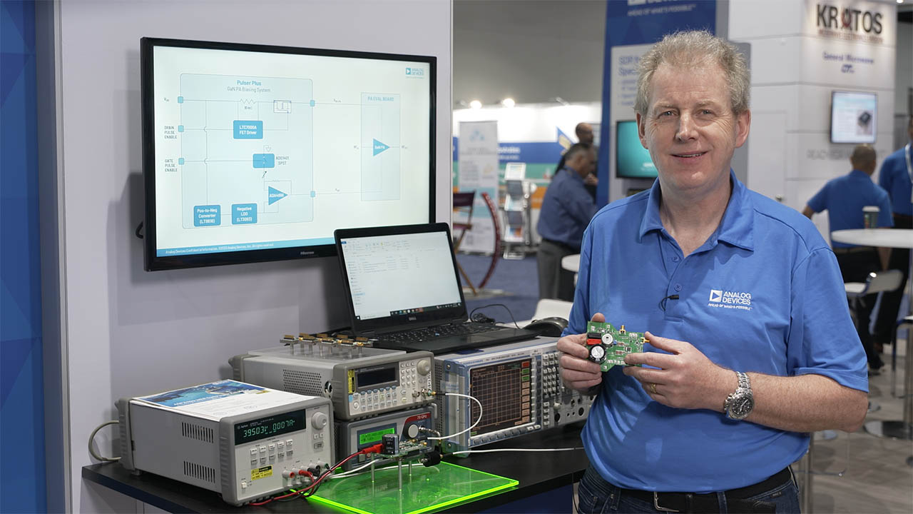
Pulser Plus Reference Design for GaN PA Biasing and Sequencing