ADL8141
RECOMMENDED FOR NEW DESIGNSGaAs, pHEMT, MMIC, Low Noise Amplifier, 14 GHz to 24 GHz
- Part Models
- 4
- 1ku List Price
- Starting From $40.30
Part Details
- Low noise, high gain LNA for Ku and K band
- Frequency range: 14 GHz to 24 GHz
- Low noise figure: 1.4 dB typical at 15 GHz to 22 GHz
- High gain: 29 dB typical at 14 GHz to 15 GHz
- Integrated AC coupling capacitors
- Integrated bias inductor
- Single positive supply: 2 V with IDQ = 25 mA
- RBIAS drain current adjustment pin
- RoHS-compliant, 2 mm × 2 mm, 8-lead LFCSP
- Wafer diffusion lot traceability
- Radiation lot acceptance test (RLAT)
- Total ionizing dose (TID)
- Radiation benchmark
- Single event latch-up (SEL)
The ADL8141 is a low power consumption, low noise amplifier that operates from 14 GHz to 24 GHz. Typical gain, noise figure, and output third-order intercept (OIP3) are 29 dB, 1.4 dB, and 18 dBm, respectively. Typical supply current is 25 mA from a 2 V supply. OIP3 and output power for 1 dB compression (OP1dB) can be increased by adjusting a supply-referenced resistor connected to the RBIAS pin. The RF input and output of the ADL8141 are internally matched and AC-coupled.
The ADL8141 is fabricated on a gallium arsenide (GaAs), pseudomorphic high electron mobility transistor (pHEMT), monolithic microwave integrated circuit (MMIC) process. The ADL8141 is housed in a RoHS-compliant, 2 mm × 2 mm, 8-lead LFCSP and is specified for operation from −40°C to +85°C.
Applications
Documentation
Data Sheet 2
User Guide 1
Application Note 2
High Dose Rate Radiation Reports 1
ADI has always placed the highest emphasis on delivering products that meet the maximum levels of quality and reliability. We achieve this by incorporating quality and reliability checks in every scope of product and process design, and in the manufacturing process as well. "Zero defects" for shipped products is always our goal. View our quality and reliability program and certifications for more information.
| Part Model | Pin/Package Drawing | Documentation | CAD Symbols, Footprints, and 3D Models |
|---|---|---|---|
| ADL8141ACPZN | 8-lead LFCSP 2 mm × 2 mm × 0.85 | ||
| ADL8141ACPZN-CSL | 8-lead LFCSP 2 mm × 2 mm × 0.85 | ||
| ADL8141ACPZN-R7 | 8-lead LFCSP 2 mm × 2 mm × 0.85 | ||
| ADL8141ACPZN-R7-CSL | 8-lead LFCSP 2 mm × 2 mm × 0.85 |
| Part Models | Product Lifecycle | PCN |
|---|---|---|
|
Sep 28, 2023 - 23_0146 Process Revision for Select Low Noise Amplifier Products |
||
| ADL8141ACPZN | PRODUCTION | |
| ADL8141ACPZN-R7 | PRODUCTION | |
This is the most up-to-date revision of the Data Sheet.
Software Resources
Can't find the software or driver you need?
Request a Driver/SoftwareTools & Simulations
S-Parameter 1
Evaluation Kits

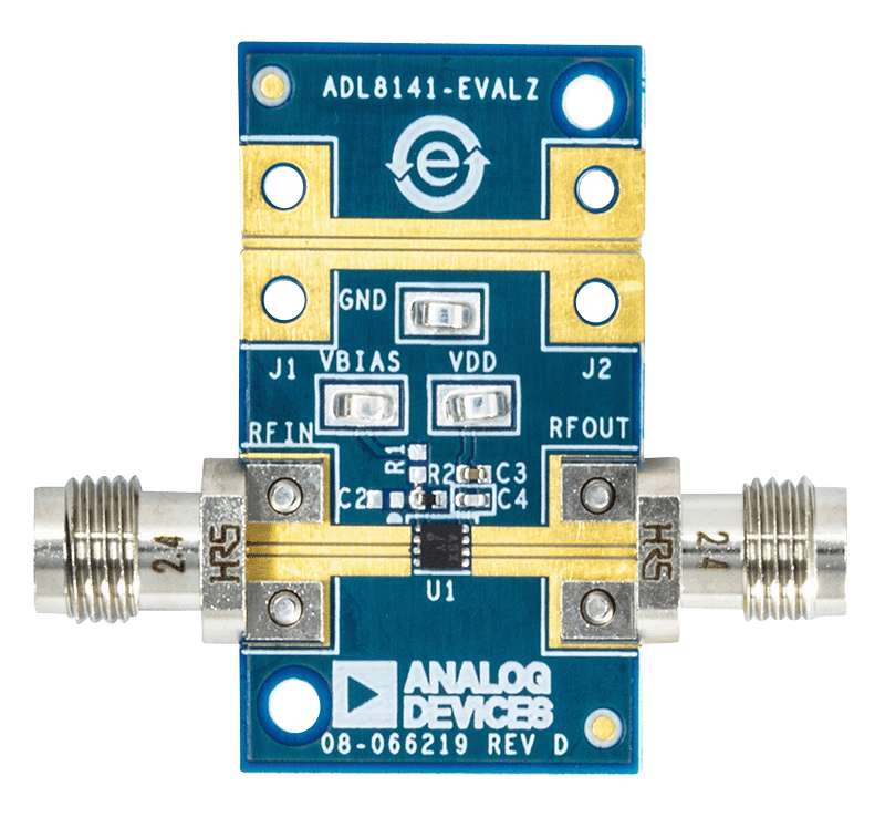

Evaluating the ADL8141 GaAs, pHEMT, MMIC, Low Noise Amplifier, 14 GHz to 24 GHz