ADL8122
RECOMMENDED FOR NEW DESIGNS10 kHz to 10 GHz, Wideband, Low Noise Amplifier
- Part Models
- 2
- 1ku List Price
- price unavailable
Part Details
- Single positive supply (self biased)
- Resistor-programmable bias setting
- Positive gain slope vs. frequency
- Wideband operation: 10 kHz to 10 GHz
- Extended operating temperature range: −55°C to +125°C
- RoHS-compliant, 2 mm × 2 mm, 8-lead LFCSP
The ADL8122 is a wideband low noise amplifier (LNA) that operates from 10 kHz to 10 GHz. Typical gain and noise figure are 17 dB and 2 dB, respectively, from 2 GHz to 6 GHz. Output power for 1 dB compression (OP1dB), output third-order intercept (OIP3), and output second-order intercept (OIP2) are 20 dBm, 33.5 dBm, and 37 dBm, respectively, from 2 GHz to 6 GHz. The nominal quiescent current (IDQ), which can be adjusted, is 95 mA from a 5 V supply voltage (VDD). The internally matched, DC-coupled RF input and output pins require external AC coupling capacitors along with a bias inductor on RFOUT. In addition, the RF input is biased through an external inductor connected between the VBIAS pin and the RFIN pin.
The ADL8122 is fabricated on a pseudomorphic, high electron mobility transistor (pHEMT) process. The device is housed in a RoHS-compliant, 2 mm × 2 mm, 8-lead LFCSP and is specified for operation from −55°C to +125°C.
APPLICATIONS
- Telecommunications
- Instrumentation
- Radar
- Electronic warfare
Documentation
Data Sheet 1
Application Note 2
ADI has always placed the highest emphasis on delivering products that meet the maximum levels of quality and reliability. We achieve this by incorporating quality and reliability checks in every scope of product and process design, and in the manufacturing process as well. "Zero defects" for shipped products is always our goal. View our quality and reliability program and certifications for more information.
| Part Model | Pin/Package Drawing | Documentation | CAD Symbols, Footprints, and 3D Models |
|---|---|---|---|
| ADL8122ACPZN | 8-lead LFCSP 2 mm × 2 mm × 0.85 | ||
| ADL8122ACPZN-R7 | 8-lead LFCSP 2 mm × 2 mm × 0.85 |
This is the most up-to-date revision of the Data Sheet.
Software Resources
Can't find the software or driver you need?
Request a Driver/SoftwareTools & Simulations
S-Parameter 1
Evaluation Kits
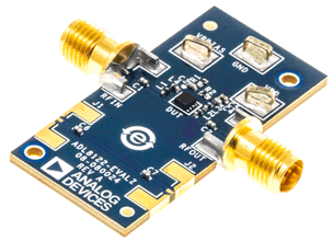


Evaluating the ADL8122 10 kHz to 10 GHz, Wideband, Low Noise Amplifier