ADL8106
RECOMMENDED FOR NEW DESIGNSGaAs, pHEMT, Low Noise Amplifier, 20 GHz to 54 GHz
- Part Models
- 4
- 1ku List Price
- Starting From $144.10
Part Details
- Gain: 21.5 dB typical at 30 GHz to 44 GHz
- Input return loss: 22 dB typical at 30 GHz to 44 GHz
- Output return loss: 23 dB typical at 30 GHz to 44 GHz
- OP1dB: 14 dB typical at 30 GHz to 44 GHz
- PSAT: 18 dBm typical at 30 GHz to 44 GHz
- OIP3: 21.5 dBm typical at 30 GHz to 44 GHz
- Noise figure: 3.0 dB typical at 30 GHz to 44 GHz
- 3 V supply voltage at 120 mA
- 50 Ω matched input and output
- Die size: 2.3 mm x 1.45 mm x 0.1 mm
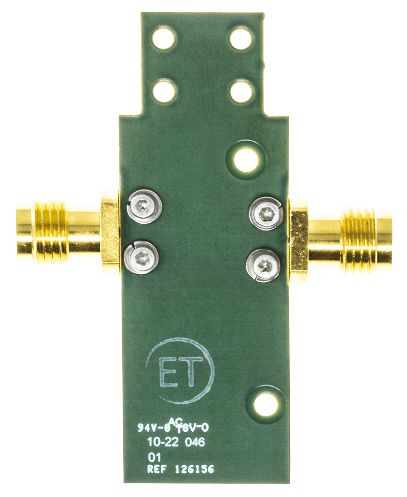
The ADL8106 is a gallium arsenide (GaAs), pseudomorphic high electron mobility transfer (pHEMT), monolithic microwave integrated circuit (MMIC), wideband low noise amplifier that operates from 20 GHz to 54 GHz. The ADL8106 provides a gain of 21.5 dB, an output power for 1 dB compression (OP1dB) of 14 dBm, and a typical output third-order intercept (OIP3) of 21.5 dBm at 30 GHz to 44 GHz. The ADL8106 requires 120 mA from a 3 V supply voltage (VDD) and features inputs and outputs that are internally matched to 50 Ω, facilitating integration into multichip modules (MCMs). All data is taken with the RFIN and RFOUT pads connected via one 0.076 mm (3 mil) wide gold ribbon bond of 0.076 mm to 0.152 mm (3 mil to 6 mil) minimal length.
Documentation
Data Sheet 2
User Guide 1
Application Note 1
Analog Dialogue 1
ADI has always placed the highest emphasis on delivering products that meet the maximum levels of quality and reliability. We achieve this by incorporating quality and reliability checks in every scope of product and process design, and in the manufacturing process as well. "Zero defects" for shipped products is always our goal. View our quality and reliability program and certifications for more information.
| Part Model | Pin/Package Drawing | Documentation | CAD Symbols, Footprints, and 3D Models |
|---|---|---|---|
| ADL8106ACEZ | 24-terminal LGA_CAV (5 mm x 5 mm x 1.60 mm) | ||
| ADL8106ACEZ-R7 | 24-terminal LGA_CAV (5 mm x 5 mm x 1.60 mm) | ||
| ADL8106CHIPS | CHIPS OR DIE | ||
| ADL8106CHIPS-SX | CHIPS OR DIE |
| Part Models | Product Lifecycle | PCN |
|---|---|---|
|
Dec 22, 2022 - 22_0300 ADL8106 Data Sheet Revision |
||
| ADL8106ACEZ | PRODUCTION | |
| ADL8106ACEZ-R7 | PRODUCTION | |
| ADL8106CHIPS | PRODUCTION | |
This is the most up-to-date revision of the Data Sheet.
Software Resources
Can't find the software or driver you need?
Request a Driver/SoftwareHardware Ecosystem
Tools & Simulations
ADIsimRF
ADIsimRF is an easy-to-use RF signal chain calculator. Cascaded gain, noise, distortion and power consumption can be calculated, plotted and exported for signal chains with up to 50 stages. ADIsimRF also includes an extensive data base of device models for ADI’s RF and mixed signal components.
Open ToolS-Parameter 2
Evaluation Kits


Evaluating the ADL8106 GaAs, pHEMT, Low Noise Amplifier, 18 GHz to 54 GHz