CN0156

Overview
Design Resources
Device Drivers
Software such as C code and/or FPGA code, used to communicate with component's digital interface.
AD9834 - Microcontroller No-OS Driver
AD983x GitHub no-OS Driver Source Code
AD9834 IIO Direct Digital Synthesis GitHub Linux Driver Source Code
Product Categories
Markets and Technologies
Parts Used
Documentation & Resources
-
The Data Conversion Handbook, 20051/2/2005
-
Fundamentals of Direct Digital Synthesis (DDS)2/14/2015PDF173 kB
-
MT-015: Basic DAC Architectures II: Binary DACs (Rev. A)3/20/2009PDF100 kB
-
CN-0156: Amplitude Control Circuit for AD9834 Waveform Generator (DDS)7/12/2013PDF316 kB
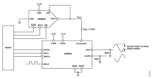
Circuit Function & Benefits
The circuit shown in Figure 1 provides a simple approach for controlling the amplitude of the output waveform of an AD9834 75 MHz low power (20 mW) waveform generator (DDS).
DDS (direct digital synthesis) devices are capable of producing sine wave, square wave, and triangular output waveforms and, therefore, serve as waveform generators.
Capability for phase modulation and frequency modulation is provided internally in the AD9834. However, in order to modulate the amplitude of the output signal, a low power DAC or digital potentiometer is required to set the full-scale current. A voltage output DAC can be used to drive the FS ADJUST pin of the AD9834 through a series resistor. This determines the magnitude of the full-scale DAC current.
The DAC used in this example is the 12-bit AD5620, a member of the nanoDAC family. The AD5620 contains an on-chip 5 ppm/°C reference, has an SPI interface, and is available in an 8-lead SOT-23 or MSOP package. The low power (2.2 mW @ 3.3 V) and small size of the AD5620 (8-lead SOT-23) provide an attractive solution for generating an amplitude modulated output from the AD9834.


Circuit Description
The circuit operates on a 3 V to 5 V single supply. Both the DAC and DDS operate with an SPI interface. The on-chip DAC for many DDS devices provides a complementary current output, IOUT and IOUTB, for the AD9834 DDS.
The reference current to the DAC is a function of the internal reference voltage, VREF, and an external resistor, RSET, which normally connects from the DAC FS ADJUST pin to ground. The reference current is equal to VREF/RSET where VREF is the internal reference of the AD9834 and has a typical value of 1.20 V. The RSET resistor has a typical value of 6.8 kΩ.
The full-scale current from the DAC is a multiple of the reference current. For example, the full-scale current of the AD9834 is

If FS ADJUST is connected to a varying voltage, VDAC, the full-scale current is

Varying VDAC varies the full-scale current and, therefore, the voltage output from the DDS device. You can provide this varying voltage by using a voltage-output DAC.
The AD5620 is a low power, small, price effective solution here. A member of the nanoDAC family, it contains an on-chip 5 ppm/°C reference and is available in an 8-lead SOT-23 or MSOP package. The output voltage of the AD5620 is 0 V to +2.5 V.
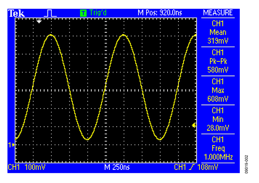
The maximum full-scale output current is reached when VDAC = 0 V (zero-scale) and the current from the AD9834 swings between approximately 0.16 mA and 3.12 mA. With the 200 Ω load resistor, the AD9834 output voltage swings between approximately 0.032 V and 0.624 V. The output voltage on the IOUT pin of the AD9834 is shown in Figure 2, where the DDS output frequency is set for 1 MHz.

Increasing the voltage output from the AD5620 reduces the full-scale output current of the AD9834. The minimum full-scale current will be reached when the voltage from the AD5620 is equal to VREF, or 1.20 V.
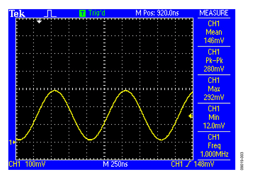
Figure 3 shows the AD9834 output voltage for a half-scale output current, where VDAC = 0.5 × VREF, or 0.6 V.

The circuit must be constructed on a multilayer PC board with a large area ground plane. Proper layout, grounding, and decoupling techniques must be used to achieve optimum performance (see MT-031 Tutorial and MT-101 Tutorial).