Abstract
I2C, or Inter-Integrated Circuit, is a commonly used serial communication protocol in establishing communication between devices, especially for two or more different circuits. I2C Primer is the most commonly used I2C. This article will provide the basic features and standards for I2C Primer, primarily to address proper usage during communication implementation. From the fundamentals of I2C, we’ll walk through the availability of its variant subsets, System Management Bus (SMBus) and Power Management Bus (PMBus), and their differences. Each of the three has dedicated functions intended to address different customer requirements.
Why Is It Important?
I2C provides benefits to the designer in establishing simple, 2-way, flexible communication between numerous nodes in a system. I2C reduces complexity by using just two bidirectional wires for transmitting and receiving information. It also allows designers to configure communication between multiple main-node system ICs. I2C also benefits developers in managing the system and power, which gives them the advantage to create a high quality product inside the best possible timeline.
“Communication works for those who work at it.”
—John Powell
Communication protocol plays a big role in organizing communication between devices. It is designed in different ways based on system requirements, and these protocols have specific, agreed-upon rules to achieve successful communication.
You’ve probably used I2C if you’ve ever built systems with LED displays, sensors, or even accelerometer modules, to name a few. I2C supports the feature of connecting multiple nodes to a single main device and multiple main devices to multiple nodes. This feature is helpful if you want to maximize having one microcontroller logging data to a single memory card or displaying text to a single LCD.
Aside from the most commonly used I2C Primer, there are two additional variations of I2C that focus on the usage for system and power applications. These are called System Management Bus (SMBus) and Power Management Bus (PMBus).
By definition, Inter-Integrated Circuit (I2C)—also known as Inter IC—is a hardware communication protocol that uses synchronous communication with a multi-main, multi-node, and serial communication bus. Synchronous communication means two (or more) devices exchanging data share a common clock line. I2C is widely used for connecting lower speed peripheral ICs to processors and microcontrollers. The I2C bus was designed by Philips to allow easy communication between components that reside on the same circuit board.
I2C Primer
Interface
Connections are minimized by using a serial data (SDA) line, a serial clock (SCL) line, and a common ground to carry all communications.


There are two wires in each I2C device:
- The SDA is the line for the main device and node to send and receive data.
- The SCL is the line that carries the clock signal. The SCL is always generated by the I2C main. The specification requires minimum periods for the low and high phases of the clock signal.
The I2C bus uses only two bidirectional lines: SDA and SCL for each device for simple inter-IC communication.


The most important hardware parts are pull-up resistors, which are used by the SDA and SCL lines. I2C compatible devices connect to the bus with open collector or open drain pins, which pull the line low. When there is no transmission of data, the I2C bus lines idle in a high state; the lines are passively pulled high. Transmission occurs by toggling the lines, by pulling low and releasing high. Bits are clocked on falling clock edges.
Open drain outputs require a pull-up resistor (Rp in Figure 2) in order to properly output high. The pull-up resistor is connected between the output pin and the output voltage (VDD in Figure 2) that is desired for a high state.
Four thousand seven hundred ohms (4700 Ω) is the most used value of pull-up resistors with typical values of VCC and VDD (5 V).
For reference, shielded 2 AWG twisted pair cables have capacitance in the range of 100 pF/m to 240 pF/m. So, the maximum bus length of an I2C link is about 1 meter at 100 kBaud, or 10 meters at 10 kBaud. Unshielded cable typically has much less capacitance but should only be used within an otherwise shielded enclosure.
Table 1 summarizes the key characteristics of I2C.
| Features | Specs |
| Wires | 2 |
| Maximum Speed | Standard mode = 100 kbps Fast mode = 400 kbps High speed mode = 3.4 Mbps Ultrafast mode = 5 Mbps |
| Synchronous or Asynchronous? | Synchronous |
| Serial or Parallel? | Serial |
| Maximum Number of Mains | Unlimited |
| Maximum Number of Nodes | 1008 |
Theoretically, the maximum number of nodes is 27 or 210 for addressing mode; however, 16 addresses are reserved for special purposes.
I2C is synchronous, so the output of bits is synchronized to the sampling of bits by a clock signal shared between the main and the node. The clock signal is always controlled by the main.
Reserved I2C Node Address
There are 16 reserved I2C addresses. These addresses correspond to one of two patterns: 0000 XXX or 1111 XXX. Table 2 shows I2C addresses reserved for special purposes..
| I2C Node Address | R/W | Bit Description |
| 0000 000 | 0 | General call address |
| 0000 000 | 1 | Start byte |
| 0000 001 | X | CBUS address |
| 0000 010 | X | Reserved for different bus format |
| 0000 011 | X | Reserved for future purposes |
| 0000 1XX | X | High speed-mode main code |
| 1111 1XX | X | Reserved for future purposes |
| 1111 0XX | X | 10-bit node address |
How Does I2C Work?
I2C data is transferred in messages, which are broken up into frames of data. The read and write protocol contains the address frame with the binary address of the node and another data frame that contains the data being transmitted, start and stop conditions, repeated start bits, read/write bits, and acknowledge/not acknowledge bits between each data frame.
Timing Specification Table
The I2C timing table is also important as it allows engineers to design ICs that are compatible with the bus requirement. Each data rate has its own timing specification to which the main and node must adhere for correct data transfer.
Table 3 shows the symbols and parameters available on a timing specification table.
| Symbol | Parameter | Units |
| fSCL | SCL clock frequency | kHz |
| tHD(STA) | Hold time (repeated) start condition | µs |
| tLOW | Low period of the SCL pin | µs |
| tHIGH | High period of the SCL pin | µs |
| tSU(STA) | Set-up time for a repeated start condition | µs |
| tHD(DAT) | Data hold time | µs |
| tSU(DAT) | Data set-up time | ns |
| tr | Rise time for SDA signals | ns |
| tf | Fall time for SDA signals | ns |
| tSU(STO) | Set-up time for stop condition | µs |


I2C Transmission Sub-Protocols
Transmission over the bus is either a read or write operation. The reading and writing protocols build upon a series of sub-protocols such as start and stop conditions, repeated start bits, address bytes, data transfer bits, and acknowledge/not acknowledge bits.
Start Condition
As the name suggests, a start condition always occurs at the start of a transmission and is initiated by the main device. This is done to wake the idling node devices on the bus. The SDA line switches from a high voltage level to a low voltage level before the SCL line switches from high to low. See Figure 4.
Repeated Start Condition
Without issuing a stop condition, a start condition can be repeated during a transmission. This is a special case, called the repeated start, and is used for changing data transmission direction, repeating transmission attempts, synchronizing several ICs, or even controlling serial memory. See Figure 5.
Address Frame
The address frame contains a 7-bit or 10-bit sequence, depending on the availability (refer to the data sheet). See Figure 6.
I2C doesn’t have node select lines like SPI, so it needs another way to let the node know that data is being sent to it, and not another node. It does this by addressing. The address frame is always the first frame after the start bit in a new message.
The main sends the address of the node it wants to communicate with to every node connected to it. Each node then compares the address sent from the main to its own address. If the address matches, it sends a low voltage ACK bit back to the main. If the address doesn’t match, the node does nothing, and the SDA line remains high.
Read/Write Bit
The address frame includes a single bit at the end that informs the node whether the main wants to write data to it or receive data from it. If the main wants to send data to the node, the read/write bit is at a low voltage level. If the main is requesting data from the node, the bit is at a high voltage level. See Figure 7.
ACK/NACK Bit
Each frame in a message is followed by an acknowledge/not acknowledge bit. If an address frame or data frame was successfully received, an ACK bit is returned to the sender from the receiving device.
Legend: For the following figures, the white box represents the node while the blue box is for the main. See Figure 8.


Data Frame
After the main detects the ACK bit from the node, the first data frame is ready to be sent. The data frame is always 8 bits long and sent with the most significant bit first. Each data frame is immediately followed by an ACK/NACK bit to verify that the frame has been received successfully. The ACK bit must be received by either the main or the node (depending on who is sending the data) before the next data frame can be sent. See Figure 9.
Stop Condition
After all the data frames have been sent, the main can send a stop condition to the node to halt the transmission. The stop condition is a voltage transition from low to high on the SDA line after a low-to-high transition on the SCL line, with the SCL line remaining high.
The SDA line switches from a low voltage level to a high voltage level after the SCL line switches from low to high. See Figure 10.
Steps of I2C Transmission: Write
For an example of I2C transmission of a write single location, see Figure 11.
Step 1
The main sends the start condition to every connected node by switching the SDA line from a high voltage level to a low voltage level before switching the SCL line from high to low.
Step 2
The main sends each node the 7-bit or 10-bit address of the node it wants to communicate with, along with the write bit.
For example, a 7-bit address is 0x2D. Adding a write bit equivalent to 0, it will be 0x5A.
Step 3
Each node compares the address sent from the main to its own address. If the address matches, the node returns an ACK bit by pulling the SDA line low for one bit. If the address from the main does not match the node’s own address, the node leaves the SDA line high.
ACK is possible by bringing the SDA line low during the ninth pulse of the SCL and floating high for NACK.
Step 4
The main sends or receives the data frame.
Step 5
After each data frame has been transferred, the receiving device returns another ACK bit to the sender to acknowledge successful receipt of the frame.
Step 6
To stop the data transmission, the main sends a stop condition to the node by switching SCL high before switching SDA high.


Steps of I2C Data Transmission: Read
Step 1
The main sends the start condition to every connected node by switching the SDA line from a high voltage level to a low voltage level before switching the SCL line from high to low.
Step 2
The main sends each node the 7-bit or 10-bit address of the node it wants to communicate with, along with the write bit.
For example, a 7-bit address is 0x2D. Adding a write bit equivalent to 0, it will be 0x5A.
Step 3
Each node compares the address sent from the main to its own address. If the address matches, the node returns an ACK bit by pulling the SDA line low for one bit. If the address from the main does not match the node’s own address, the node leaves the SDA line high.
Step 4
After the initial start, addressing, and acknowledge, since the main already knows its node and the address to point to, some devices have a repeated start condition to clean the transaction.
Note: For reading purposes only!
Step 5
The main sends each node the 7-bit or 10-bit address of the node it wants to communicate with, along with the read bit.
For example, a 7-bit address is 0x2D. Adding a read bit equivalent to 1, it will be 0x5B.
Step 6
Each node compares the address sent from the main to its own address. If the address matches, the node returns an ACK bit by pulling the SDA line low for one bit. If the address from the main does not match the node’s own address, the node leaves the SDA line high.
Step 7
After the ACK bit, the main receives the data frame from the node.
Step 8
After each data frame has been transferred, the main returns another ACK bit to the sender to acknowledge successful receipt of the frame, or the main returns a NACK if the read request is already done.
Step 9
To stop the data transmission, the main sends a stop condition to the node by switching SCL high before switching SDA high.
Single Main with Multiple Nodes
Because I2C uses addressing, multiple nodes can be controlled from a single main. With a 7-bit address, 128 (27) unique addresses are available. Using 10-bit addresses is uncommon but provides 1024 (210) unique addresses. To connect multiple nodes to a single main, wire them with 4.7 kΩ pull-up resistors connecting the SDA and SCL lines to VCC.
Multiple Mains with Multiple Nodes
Multiple main devices can be connected to a single node or multiple nodes. The problem with multiple main devices in the same system comes when two mains try to send or receive data at the same time over the SDA line.
To solve this problem, each main needs to detect if the SDA line is low or high before transmitting a message.
If the SDA line is low, this means that another main has control of the bus, and the main should wait to send the message. If the SDA line is high, then it’s safe to transmit the message. To connect multiple mains to multiple nodes, use the diagram shown in Figure 13, with 4.7 kΩ pull-up resistors connecting the SDA and SCL lines to VCC.


Arbitration
Several I2C multi-main devices can be connected to the same I2C bus and operate concurrently. By constantly monitoring the SDA and SCL for start and stop conditions, they can determine whether the bus is currently idle or not. If the bus is busy, the main device delays pending I2C transfers until a stop condition indicates that the bus is free again.
However, it may happen that two main devices start a transfer at the same time. During the transfer, the mains constantly monitor the SDA and SCL. If one of them detects that SDA is low when it should be high, it assumes that another main is active and immediately stops its transfer. This process is called arbitration. Both mains generate a start bit and proceed with their transmissions.
If the mains happen to choose the same logic levels, nothing happens.
As soon as the mains attempt to impose different logic levels, the main driving the signal low is proclaimed the winner; the loser detects the logic mismatch and abandons its transmission.
Take a moment to appreciate the simplicity and efficacy of this arrangement:
- The winner continues its transmission without interruption—no corrupted data, no driver contention, no need to restart the transaction.
- Theoretically the loser could monitor the node address during the arbitration process and make a proper response if it happens to be the addressed node.
- If the competing mains are both requesting data from the same node, the arbitration process does not unnecessarily interrupt either transaction—no mismatch will be detected, and the node will output its data to the bus such that multiple mains can receive it.
Clock Stretching
This is also referred to as clock synchronization.
Note: The I2C specification does not specify any timeout conditions for clock stretching—that is, any device can hold down SCL if it likes.
In I2C communication protocol, the clock speed and signals are always generated by the main device. The signal generated by the I2C main device provides synchronization between the main and node connection.
There are instances where a node or subnode is not fully working and needs to slow down prior to receiving the generated clock from the main. This is accomplished through a mechanism known as clock stretching.
During the clock stretching period, in order to reduce the bus speed, the node is allowed to hold down the clock. While on the main side, it is necessary that, after its high state, the clock signal must be read back. Then it must wait until the line has reached the high state.
Bandwidth
While clock stretching is a common practice, there is an effect on the bandwidth side. In using clock stretching, the total bandwidth among the shared bus might be significantly decreased. Bus performance must still be reliable and fast even using this technique. It is necessary to cover the estimated effects of using clock stretching, especially on I2C buses shared by multiple devices.

Clock stretching allows an I2C node device to force the main device into a wait state. A node device may perform clock stretching when it needs more time to manage data—for example, to store received data or prepare to transmit another byte of data. This typically occurs after the node device has received and acknowledged a byte of data.
Which I2C Node Devices Need Clock Stretching?
Whether or not clock stretching is needed depends on the functions of the node device. Here are two examples:
- A processing device, such as a microprocessor or a microcontroller, may need additional time to process an interrupt, receive and manage data, and perform the appropriate function(s).
- A simpler device, such as an EEPROM, does not process data internally, so it does not need clock stretching to perform any of its functions.
I2C Data Sheet Sample Overview
There are different approaches in terms of creating a data sheet depending on different companies and manufacturers. As a starter, Figure 13 shows a sample data sheet and basic I2C details including registers and electronic specifications.

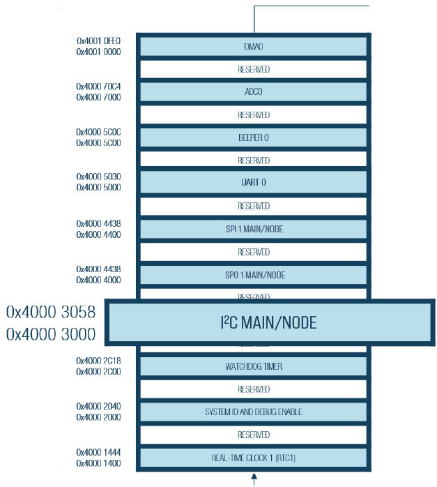
Table 4 shows the most used I2C registers. Names and descriptions may vary depending on the data sheet, but the functionality and usage is common.
| Name | Description |
| I2C_ADDR1 | Main address byte 1 |
| I2C_ADDR2 | Main address byte 2 |
| I2C_BYT | Start byte |
| I2C_ID | Node address device ID |
| I2C_MCTL | Main control |
| I2C_MRX | Main receive data |
| I2C_SCTL | Node control |
| I2C_SRX | Node receive |
| I2C_STAT | Main and node FIFO status |
The creation of I2C may vary depending on usage. Table 5 shows a sample of basic I2C driver API requirements.
| Main | Node |
| Initialization |
|
| Tx Handler | Tx Handler |
| Rx Handler | Rx Handler |
| Event Interrupt |
|
| Error Interrupt |
|
SMBus
SMBus is known to be used in applications that require critical monitoring of parameters. It is most commonly used in computer motherboards and embedded system applications. It has additional monitoring specifications for temperature, supply voltage, fan monitor, and/or control integrated chips.
The SMBus is a 2-wire bus that is similar to the I2C bus that was developed by Philips in the 1980s. The two main signals are the clock, or SMBCLK, and data, or SMBDAT. The I2C primer and SMBus are compatible with each other, but there are notable differences such as:
- The SMBus logic level thresholds are fixed and not proportional to a device’s supply voltage. This allows devices with different supply voltages to operate on the same primer. For example, one SMBus might have devices powered from 1.8 V, 3.3 V, and 5 V.
- They both operate on the same speed up to 100 kHz, but the I2C primer has 400 kHz and 2 MHz versions.
- The SMBus provides for a minimum clock speed and limits the amount the clock may be stretched in one transaction. A violation of the timeout limits causes all SMBus devices to reset their I/O logic to allow the bus to restart. This enhances the robustness of the bus.
- The timeout for both is also different. The I2C primer has no timeout while the SMBus has a timeout—consider 35 ms for a 10 kHz minimum clock speed.
- Packet error checking (PEC) was originally defined for SMBus. A packet error code byte is added at the end of each transaction.
- Some of the remaining differences involve transfer types, alert line, suspend line, and power down or up.
It is an explicit requirement that an SMBus device must acknowledge (ACK) its own address every time it is received, regardless of what else the device may be doing. This assures that a main device can accurately determine what devices are active on the bus.
All SMBus transactions are carried out through one of the specified SMBus protocols.
The SMBus includes an optional signal, SMBALERT#, that node devices can use to quickly notify the main or system host that it has information for the main, such as reporting a fault condition.


SMBus Pull-Up Circuitry


SMBus Address
SMBus addresses are 7 binary bits long and are conventionally expressed as 4 bits followed by 3 bits followed by the letter b—for example, 0001 110b. These addresses occupy the high 7 bits of an 8-bit field on the bus. The low bit of this field, however, has another semantic meaning that is not part of an SMBus address.

Figure 18. Node address.
A 7-bit destination address is sent from the main to one or more devices (such as with the general call address) on the bus.
Note the start and stop conditions are transitions, not bits, and are shown without a bit count number above the symbol. When shown in a transaction diagram, the repeated start is also a transition, not a bit, and is shown without a bit count above the symbol.


SMBus Timing Measurements
| Symbol | Parameters | Units |
| fSMB | SMBus operating frequency | kHz |
| tBUF | Bus free time between stop and start condition | µs |
| THD-STA | Hold time after (repeated) start condition | µs |
| TSU-STA | Repeated start condition set-up time | µs |
| tSU(STO) | Stop condition set-up time | µs |
| tHD(DAT) | Data hold time | ns |
| tSU(DAT) | Data set-up time | ns |
| tTIMEOUT | Detect clock low timeout | ms |
| tLOW | Clock low period | µs |
| tHIGH | Clock high period | µs |
PMBus: Power Management Redefined
In addition to SMBus comes a variant, the PMBus, which is an open standard power management protocol. This flexible and highly versatile standard allows for communication between devices based on both analog and digital technologies, and provides true interoperability, which will reduce design complexity and shorten time to market for power system designers.
PMBus is used in digital management of power supplies with power control and management components. It has commands and structures to support the requirement for power management. This means both I2C primer and PMBus are compatible and interoperable on the electrical requirements and command semantics.
One of the essential parameters in power management is monitoring of overvoltage level, and PMBus provides a command for setting and reading it. By adding to the available features of I2C primer and SMBus, PMBus acts as a protocol layer on top of the existing standards, especially the SMBus.
The I2C specification only describes the physical layer, timing, and flow control of a 2-wire bus. The I2C specification does not describe the format of messages (like the SMBus protocols) and does not describe the content of the messages.
The PMBus specification is a complete power management protocol. It includes how to get the bits and bytes from one device to another (that is, transport); it also describes a command language that gives meaning to those bits and bytes.
Addressing
For redundant systems there are up to three signals to set the address location of the power supply once it is installed in the system: Address2, Address1, and Address0. For non-redundant systems, the power supply device address location should be B0h.
Hardware
The device in the power supply shall be compatible with SMBus 2.0 high power specifications for I2C VDD-based power and drive (for VDD = 3.3 V). This bus shall operate at 3.3 V.
Power Sourcing
The device in the power supply shall be compatible with SMBus 2.0 high power specifications for I2C VDD-based power and drive (for VDD = 3.3 V). This bus shall operate at 3.3 V.
Pull-Ups
Only weak pull-up resistors shall be on the SCL or SDA lines inside the power supply. The main pull-up resistors are provided by the system and may be connected to 3.3 V or 5 V. For the system design, the main pull-ups shall be located external to the power supply and derive their power from the standby rail.
Data Speed
The PMBus device in the power supply shall operate at the full 100 kbps SMBus speed and avoid using clock stretching as much as possible, as it can slow down the bus.
Summary
Table 8 provides a general view and summary in terms of specifications: signaling, timing, and electrical among I2C Primer, SMBus (both for high and low power), and PMBus.
How Are I2C Primer, SMBus, and PMBus Related?
Originally developed to facilitate battery management systems, SMBus uses I2C hardware but adds second-level software, which ultimately allows devices to be hot swapped without restarting the system. PMBus extends SMBus by defining a set of device commands specifically designed to manage power converters, exposing device attributes such as measured voltage, current, temperature, and more. In general, I2C primer, SMBus, and PMBus devices can share a bus without any major issues.
I2C, SMB, PMB Advantages
- Only uses two wires
- With ACK/NACK bit
- Well-known protocol
- Supports multiple main devices and multiple nodes
- Hardware is less complicated than UART
- Widely used method
Disadvantages
- Slower data transfer rate than SPI
- Size of the data frame is limited to 8 bits
- More complicated hardware needed to implement than SPI


| Addresses Used | Main Addressing Used for Most Server Power Supplies with Two Addressing Pins | Additional Addresses If Three Addressing Pins Are Provided on the Power Supplies | ||||||
| System Addressing Address2/Address1/Address0 | 0/0/0 | 0/0/1 | 0/1/1 | 0/1/1 | 1/0/0 | 1/0/1 | 1/1/0 | 1/1/1 |
| PMBus Device Read Addresses | B0h/B1h | B2h/B3h | B4h/B5h | B6h/B7h | B8h/B9h | BAh/BBh | BCh/BDh | BEh/BFh |
Use Cases
- Sensor reading
- Sensor writing
- EEPROM, temperature sensor, touch screen, proximity
- Transmitting and controlling user directed actions
- Communicating with multiple microcontrollers
- Consumer electronics
- System management
- Power management
- Debugging
| Specification | I2C Primer |
SMBus High Power | Low Power |
PMBus | ||
| Signaling | Packet Error Checking (Optional) SMBALERT (Optional) Block Size Limit |
— — — |
— — 32 bytes |
— — 32 bytes |
— — 255 bytes |
| Timing | Data Rate: Standard Mode Fast Mode Fast Mode Plus High Speed Mode Clock Speed Bus Timeout Bus Main Request Delay (Min) SCL Hold Time (Max) Data Hold Time (Min) |
100 kbps 400 kbps 1 Mbps 3.4 Mbps 0 Hz to 3.4 MHz — — — — |
100 kbps — — — — 10 kHz to 100 kHz 25 ms to 35 ms 50 μs — 2 ms 300 ns |
100 kbps — — — — 10 kHz to 100 kHz 25 ms to 35 ms 50 μs — 2 ms 300 ns |
100 kbps 400 kbps — — 10 kHz to 400 kHz 25 ms to 35 ms 50 μs — 2 ms 300 ns |
| Electrical | Capacitance Load per Bus Segment (Max) Rise Time (Max) Pull-Up Current at 0.4 V (Max) Leakage Current per Device (Max) VIL Input Logic Low Threshold (Max) VIH Input Logic High Threshold (Min) VOL Output Logic Low Threshold (Max) |
400 pF 1 μs at 100 kHz, 300 ns at 400 kHz 3 mA (standard and fast mode) ±10 μA 0.3 VDD or 1.5 V 0.7 VCC or 3 V 0.4 V |
400 pF 1 μs 4 mA ±10 μA 0.8 V 2.1 V 2.4 V |
— 1 μs 350 μA ±5 μA 0.8 V 2.1 V 0.4 V |
400 pF 1 μs at 100 kHz, 300 ns at 400 kHz 4 mA ±10 μA 0.8 V 2.1 V 0.4 V |
References
“Advantages and Limitations of I2C Communication.” Total Phase, August 2016.
Afzal, Sal. “I2C Primer: What Is I2C? (Part 1).” Analog Devices, Inc.
Afzal, Sal. “I2C Timing: Definition and Specification Guide (Part 2).” Analog Devices, Inc.
Campbell, Scott. “Basics of the I2C Communication Protocol.” Circuit Basics.
I2C Quick Guide Analog Devices, Inc.
“I2C—What’s That?” I2C Bus.

