How to Accurately Calculate Overcurrent in High-Side Current-Sense Amplifiers
摘要
Recently, an engineer asked for a solution to provide high-side monitoring of a 20A load with an accurate overcurrent detection threshold better than 5%. There are no easily accessible off-the-shelf solutions that offer the ability to use a low-value sense resistor with less than 5% accuracy! Why 5%? Would 10% be OK? For a 20A load, a 10% current limit would cause the trip threshold to be 18A minimum or 22A maximum, a much wider margin than would be acceptable. What are the factors involved that make 5% so difficult? In this application note, we discuss the challenges of achieving 5% accuracy, and present a solution that delivers the required accuracy for a high-side current-sense amplifier over-current protection scheme.
Overview
A current-sense amplifier (CSA) can be designed using a variety of topologies, two of which are shown in Figures 1 and 2. In Figure 1, an operational amplifier (op amp) is configured as a differential amplifier used to amplify the differential voltage developed across a current-sense shunt resistor. There are some applications where low-side current-sensing can be used with limitations; however, these cases will not be discussed in this application note. Refer to Maxim application note 746, "High-Side Current-Sense Measurement: Circuits and Principles" for more details on low-side current-sensing vs. high-side current-sensing.
The main limitation of the differential amplifier topology is the resistor ratio match of R1 to R4 that sets the differential gain and the common-mode gain error. Two equations dictate the main source of accuracy errors for the circuit. Equation 1 is the equation for the gain of Figure 1 and Equation 2 details the common-mode gain error. Equation 3 is used to calculate VOUT for Figure 1.


VOUT = Gd × ILOAD × RSENSE + Vcm × Gcm
The overall error for measuring current would be greater than 5% when using 1% resistors for R1 to R4 and calculating the errors with worst-case tolerances. As a result, there would be a need for lower tolerance resistors at a higher expense. The main drawback of this approach is the requirement for precision resistors with tight tolerance of the ratio values of R4/R3 and R2/R1 to overcome the error sensitivity to higher common-mode voltages.
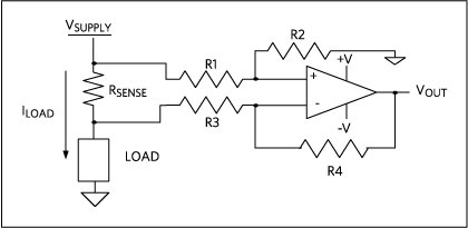
Figure 1. Op amp-based differential amplifier.
Figure 2 shows another common topology for designing CSAs. With this approach, a current-sense shunt resistor is still used to sense the load current. The voltage developed across the sense resistor is then mirrored across R1and this current is transferred to ROUT. The CSA voltage output is then:

When we rearrange the equation, we see that:

In this configuration, the gain is simply the ratio of ROUT/R1. During the manufacturing process, the ratio error can be easily trimmed out. This topology greatly eases the requirement for tightly matched resistor ratios, as is important for the differential amplifiers approach depicted in Figure 1. As a result, we can substantially reduce the common-mode voltage errors that were found in the previous approach. To minimize errors, R2 = R1 to help cancel out any offset error stemming from input bias currents.
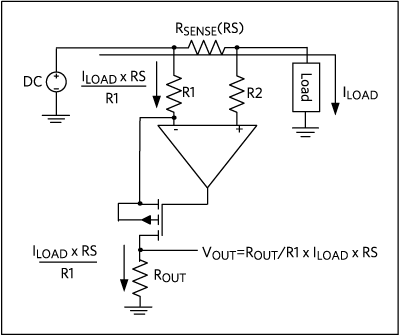
Figure 2. Maxim current-sense topology.
Steps Toward Designing a Solution
Designing a solution that minimizes overall measurement error for high-side CSAs starts with a basic circuit diagram, as shown in Figure 3.
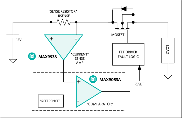
Figure 3. Overcurrent detection circuit.
There are various ways to design a circuit to solve the same problem. The solution depicted in Figure 3 uses more than one IC. However, before embarking on the process of designing a two-chip solution, let's consider the MAX4373, which integrates most of the current-detection functionality needed (Figure 4).
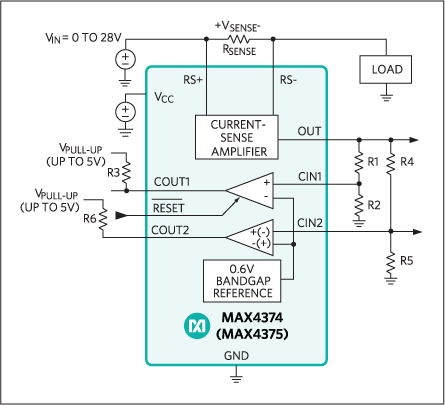
Figure 4. MAX4373/MAX4374/MAX4375 functional circuit diagram.
The MAX4373 integrates a CSA, a 0.6V internal reference, and a single comparator with a latched output to support a smaller overall footprint. The latched comparator output with its reset input makes it possible to control an external p-channel MOSFET, which, in turn, eases implementation compared to the solution depicted in the Figure 3 block diagram. Figure 5 shows a typical overcurrent protection circuit diagram. Voltage inputs greater than 5V call for a level-shifting circuit between COUT1 and the MOSFET gate. This is required to control the external MOSFET as 5V is the maximum pullup voltage on COUT1.
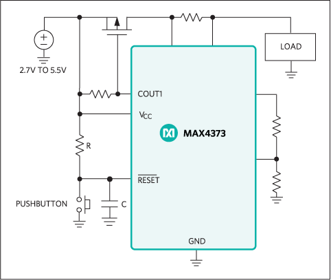
Figure 5. MAX4373 overcurrent protection circuit.
While the MAX4373 presents an interesting option, it is best to conduct a side-by-side comparison to determine the optimal solution. After inputting all the required parameters into a spreadsheet, it is clear that the MAX4373 solution would not provide better results than the 5% worst-case accuracy. Performing a similar exercise with the MAX9938, we find that this option offers an even better solution to minimize the accuracy error.
| Specification | MAX9938/MAX9053A | MAX4373 |
| CSA input offset over temp | 600µV | 2mV |
| CSA gain error over temp | ±0.6% | ±2.7% |
| CSA -3dB BW G = 100 | 30kHz | 110kHz |
| Comparator reference initial accuracy (+25°C) | ±10mV | ±10mV |
| Reference tMIN - tMAX | 2.495V min/2.5045V max | 0.586V min/0.614V max |
| Worst-case comparator input offset voltage | ±7mV | N/A |
| Comparator propagation delay | 450ns | 4µs typ |
This application note does not detail the design and selection of the MOSFET and MOSFET driver/fault logic circuit, since the document is primarily about the accuracy of detecting overcurrent. To learn techniques to control the MOSFET, refer to Maxim Application Notes 4501, 265, 4415, and 2015.
The design requirements for our solution are as follows:
- V supply = 12V ±10%, (10.8V min/13.2V max)
- Maximum load current = 20A
- Maximum current limit accuracy at 20A = ±5% or ±1A
Response time is also critical, since it could also impact accuracy and circuit protection reliability. Note that the comparator selected for this solution has a very fast response time as outlined in Table 1.
Selecting the Current-Sense Shunt Resistor
It is critical to determine the optimum value for the current-sense resistor (RSENSE). Larger RSENSE values increase the series IR voltage drop and power loss; however, this would also minimize the effect of the offset voltage error, as shown in Table 2. For designs that mandate minimal voltage and power loss, use the lowest RSENSE value possible while staying under the overall accuracy target. Table 2 features a quick overview outlining the CSA voltage output error due to CSA offset voltage and the RSENSE value. There is, however, a trade-off here between choosing a smaller current-sense resistor at the expense of increasing the gain and a higher value current-sense resistor at the expense of using a larger higher power current-sense resistor (RSENSE) that minimizes the effect of input offset voltage. High current-sensing applications such as this one can produce substantial I2R power losses in RSENSE. For this design, a 0.00125Ω sense resistor and CSA gain of 100 offers a good compromise between power dissipation and output error. Note that Table 2 was constructed using the desired maximum output current of 20A and the voltage trip level is set by the comparator reference voltage of 2.5V. For the MAX9938, CSA gain options are 25, 50, 100, and 200. Note that for a 1.25V reference, the required gain could be decreased by a factor of two using the same sense resistor. For this example, we stay with a 2.5V reference.
| CSA gain | VSENSE (F.S) (2.5V/gain) |
RSENSE (RS) (VSENSE/ILOAD) |
PD(RS) (W) | CSA VOUT error due to MAX9938 VOS (±600V over temp) with ideal CSA gain (%) |
| 25 | 0.100 | 0.005 | 2 | 0.6 |
| 50 | 0.050 | 0.0025 | 1 | 1.2 |
| 100 | 0.025 | 0.00125 | 0.5 | 2.4 |
| 200 | 0.0125 | 0.000625 | 0.25 | 4.8 |
As previously noted, start with a CSA gain of 100 to minimize the voltage drop and power loss across the sense resistor. To design a circuit with the best accuracy and small footprint, we use the MAX9053A comparator with integrated precision reference and the MAX9938 precision CSA. The MAX9938 uses a similar topology shown in Figure 2. Many other suitable CSAs with even lower DC errors could have been used for this design. For example, the MAX44284 would have been another excellent choice, featuring a maximum input offset voltage of ±27µV and a maximum gain error of 0.26%. Using an RS value of 0.00125Ω, the ideal linear response for the CSA is 125mV/A, yielding a CSA output of 2.5V for a 20A load. Note that available standard value current-sense resistors can differ from those generated in Table 2. Simply use these values for an ideal trip point of 20A without adjustment. Use the design spreadsheet to enter other values and quickly recalculate the new trip points. Table 3 and Table 4 show the data sheet errors for the CSA and comparator. These parameters are used in the error budget spreadsheet.
| Sense resistor tolerance (%) | 1 |
| Sense resistor temperature drift (ppm) | 10 |
| Current-sense amp gain error over temp (%) | ±0.6 |
| Current-sense amp offset error over temp (µV) | ±600 |
| Reference temperature coefficient (ppm) | 30 |
| Initial reference tolerance error (V) | ±0.010 |
| Comparator offset error (V) | ±0.007 |
The equations below are used in the spreadsheet. The voltage output for the CSA is defined in Equation 4.
VOUT = (Gain ±GE × VSENSE(temp) ±(Gain × VOS) (Eq. 4)
Additionally, the current-sense resistor tolerance and drift over temperature need to be considered in calculating the total error relative to the CSA.


VSENSE(temp) = Load Current × RSENSE(temp)
Equations 8 to 10 are needed for calculating errors due to comparator with internal reference.
VREF(25°C) = VREF + ±Initial Reference Tolerance

ACTUAL CURRENT LIMIT THRESHOLD ERROR (Vtrip) = Vref(temp) + Voffset
Equation 11 factors in the actual comparator trip level and the CSA errors and calculates the actual current limit trip point

Saving Time with Design Spreadsheets
Using spreadsheets to calculate errors can save valuable time, particularly when changes are needed. Figure 6 shows a spreadsheet used to calculate total error based on worst-case errors pulled from the data sheet. The root sum of squares (RSS) analysis, where total error is the square root of the sum of squares of the individual errors, was not used. RSS is based on the idea that while adding two distributions of random (normally distributed or Gaussian) measurements, the standard deviation of the resulting distribution is equal to the square root of the sum of the squares of the standard deviations of the initial distributions. Because the individual error sources are not correlated, the RSS method can be more realistic than the worst-case method (as in the case of a CSA). For this spreadsheet, calculate the voltage output of the CSAs based on worst gain error, offset error and sense resistor tolerance, and drift over temperature. Next, calculate the worst-case comparator trip level and perform an error calculation based on these two values. Ideally, the error is higher than that of the RSS method. Because the calculated error in this example is less than 5% using worst-case errors, the actual real error should be less than the calculated worst-case error. Note that any errors due to CMMR are not included, since these errors are insignificant based upon datasheet inspection. Maxim application note 5095, "DC Error Budget Calculator Simplifies Selection of Optimal Current-Sense Amplifiers" provides another good document that calculates the DC error budget in CSAs using the RSS method. The Figure 6 spreadsheet also includes the errors from the comparator used to determine the overcurrent trip point. Application Note 5095 provides a useful online spreadsheet that can be accessed here.
| Comparator Accuracy | ||
| Enter in These Values for Comparator | ||
| Delta Temp for Drift | 40 | C |
| Reference | 30 | ppm |
| NOMINAL | 2.5 | V |
| Worst-Case Initial Tolerance | 0.0008 | V |
| ±Worst-Case Comparator Offset | 0.0007 | V |
| Calculated Comparator Measurement Errors | ||
| Drift Error | 0.12 | % |
| Comparator with Threshold | 0.72 | % |
| Comparator Trip Point | 2.518 | V |
| Comparator Trip Level Error (referred to as the I-sense output) | -0.018 | V |
| Current Amp Accuracy | ||
| Enter in These Values for CS Amp | ||
| Current-Sense Resistor RS | 0.00125 | Ohms |
| Current-Sense Resistor Tolerance | -1 | |
| Current-Sense Resistor Temp Co | 50 | ppm |
| Delta Temp for Drift | 40 | |
| Actual Current-Sense Resistor (RS) Value | 0.0012500750 | |
| Calculated Resistor Power Dissipation | 0.50399 | W |
| Ideal Current-Sense Amplifier Gain | 100 | V/V |
| Load Current | 20.00000 | Amps |
| Current-Sense Amplifier Datasheet Gain Error | 0.6 | %s |
| Current-Sense Amplifier Datasheet Offset Error | 600 | µV's |
| Calculated CS Amp Measurement Errors | ||
| Current-Sense Ideal Vout | 2.5 | Volts |
| Current-Sense Actual Vout = Act Vsense × Act G ± Act G x Vosh | 2.5644703 | Volts |
| Current-Sense Vin (Vsense) Ideal | 0.025 | Volts |
| Current-Sense Vin (Vsense) Actual = Act RS × Load Current | 0.0251995 | |
| Current-Sense Actual Gain | 99.4 | V/V |
| Total Current Amp Voltage Error (referred to as I-sense output) | 0.06289545 | V |
| Actual Current Limit = Vtrip - (G x Vos)/G/Rsenseh | 19.6289545 | A |
| Trip Point Error | 1.8552 | % |
Figure 6. Error budget design spreadsheet.
Summary
CSAs can be used in a wide range of applications. To minimize overall measurement error, it is essential to understand the application trade-offs when designing with CSAs. In this application note, we defined the error sources for the current limit circuit, organizing them in an easy-to-use spreadsheet.
最新视频 21


