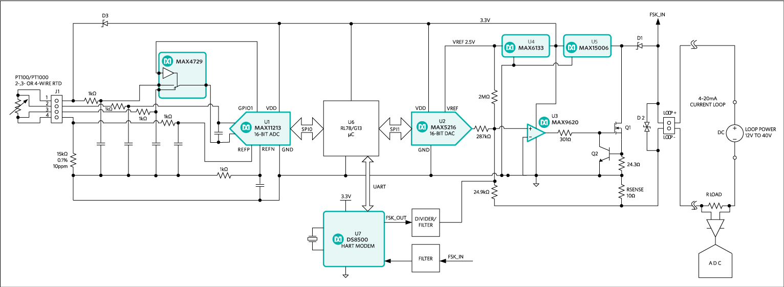
Block diagram of the Novato smart sensor transmitter is shown in Figure 1.
Figure 1. Novato (MAXREFDES16#) block diagram.
The signal chain contains the MAX11213 (U1), 16-bit delta-sigma ADC with programmable gain and GPIO, the RL78/G13 Renesas' microcontroller with 128kB flash memory (U6), and the 4–20mA current loop transmitter built on the MAX5216 and MAX9620 (U2 and U3). The DS8500 modem (U7) provides digital interface utilizing HART protocol over 4–20mA current loop. The MAX15006 (U5) and MAX6133 (U4) provide power and reference voltage to the entire circuitry.
For more detailed information about 4–20mA current loop transmitter refer to reference schematic 5610, "High-Performance, High-Accuracy 4-20mA Current-Loop Transmitter Meets Toughest Industrial Requirements."
This design uses a ratiometric measurement of sensor resistance according to the ADC transfer function (Eq. 1 and Eq. 2):
(VAINP - VAINN) = IRTD × RRTD is a voltage drop on RTD,
VREF = IRTD × RREF is a voltage drop on reference resistor RREF
Equation 1 can be rewritten as:
ADCcode = RRTD/(RREF/gain) × (216 - 1) (Eq. 2)
Then the ADC code is converted into temperature data according to the Callendar-Van Dusen equation (Eq. 3):
R(T) = R0(1 + A × T + B × T2 – 100 × C × T3 + C × T4) (Eq. 3)
where
R(T) is RTD resistance at temperature T (°C)
R0 is RTD resistance at 0°C
A, B, and C constants are derived from experimentally determined parameters and regulated by the IEC751 standard; they also must be provided by RTD manufacturers
For PT100 and temperature coefficient of resistance: α = 0.003850 [α = (R100 – R0)/(100 × R0)]
A = 3.90830 × 10⁻³
B = -5.77500 × 10⁻⁷
C = 4.18301 × 10⁻¹² for -200°C ≤ T ≤ 0°C
C = 0 for 0°C ≤ T ≤ 850°C.
Temperature T can be calculated by solving quadratic equation if we ignore coefficient C = 4.18301 × 10⁻¹² for negative temperature (Eq. 4):
T(°C) = (-A + √(A2 - 4B(1 - RRTD/R0)))/2B (Eq. 4)
where
RRTD = (ADCcode × RREF)/((216 - 1) × gain)
After that, temperature is converted into 4–20mA loop current using equation Eq. 5:
Thus, loop current is proportional to the temperature (T).
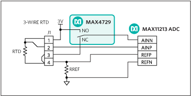
The MAX11213 ADC allows auto compensation of the sensor wire resistance by measuring that resistance during the calibration procedure and continuously subtracting that value from each conversion result. The wire resistance compensation technique is a one-step process called system offset calibration.
In normal operation the ADC measures the voltage drop between points 2 and 3 of connector J1, see Figure 2. For the offset calibration, the MAX4729 switches into the NO (normally opened) position and the ADC measures the voltage between points 1 and 2 of connector J1. In other words, the ADC measures wire resistance and automatically stores that value into the System Offset Calibration register.
Figure 2. Sensor's wire measurement using the MAX4729 mux.
The central control unit (CCU) or programmable logic controller (PLC) can convert the loop current back to the temperature using Eq. 6:
The Novato (MAXREFDES16#) smart sensor transmitter board is loaded with the firmware that supports any RTD, from PT100 to PT1000. Selection of the right sensor can be done during calibration.
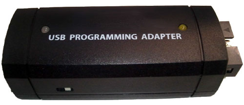
Calibration of the sensor is easy with the supporting Novato calibration software and USB-to-UART programming adapter, Figure 3.
Figure 3. Novato USB-to-UART programming adapter.
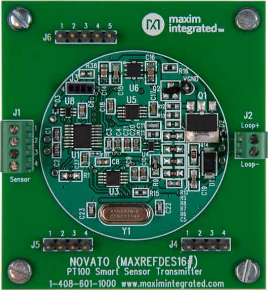
Figure 4. Novato smart sensor transmitter.
The programming adapter is connected to a PC through the USB port, and to the Novato board J4 header with a 2-wire UART interface, Figure 4.
Connect the Novato board to the 4–20mA current loop and supply the power according to the block diagram in Figure 1.
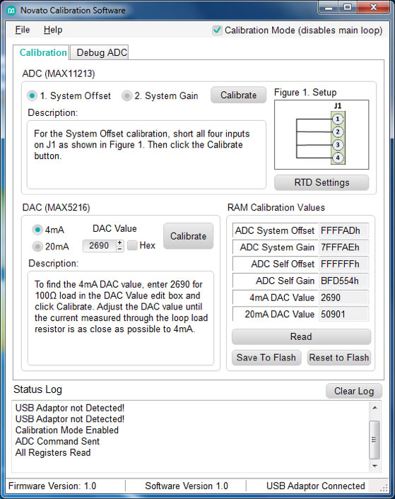
Plug in the USB-to-UART programming adapter to the PC and start the Novato calibration software, Figure 5. Wait until the PC enumerates the USB device and the software reports that the USB adapter is connected.
Figure 5. Novato calibration GUI.
The GUI is user friendly and easy to navigate. Just follow the tips in the Status box.
Step 1: Disable main loop to allow communication to the sensor by selecting the Calibration Mode checkbox. Note all functions are disabled (grayed) until Calibration mode is enabled.
Step 2: Select RTD.
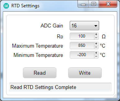
In the Calibration tab, clicking the "RTD Settings" button opens the RTD Settings window, Figure 6. Then select the appropriate R0 resistance at 0°C of RTD, which is going to be connected to the Novato board, e.g. 100Ω, gain, max and min temperature.
Figure 6. RTD Settings pop up window.
Use the appropriate settings from Table 1 and click the Write button. Click the Read button to verify the correct parameters are written.
Table 1. RTD Parameters
Parameter
PT100
PT200
PT500
PT1000
R0 (Ω)
100
200
500
1000
Gain
16
16
8
4
Max. Temperature (°C)
850
630
630
630
Min. Temperature (°C)
-200
-200
-200
-200
Step 3: Perform system offset calibration.
Short J1.1, J1.2, J1.3, and J1.4 of the sensor input connector. Select the System Offset radio button and click the Calibrate button.
Tip: Press the Read button to check how the values are changed during calibration.
Step 4: Perform system gain calibration.
Short J1.1, J1.2, and J1.4; connect J1.3 to the VGND test point. Select the System Gain radio button and click the Calibrate button.
Step 5: Perform 20mA loop current calibration.
Select the 20mA radio button, enter a value in the DAC Value edit box and click the Calibrate button. This value must be found manually by selecting a DAC code and measuring the loop current by external digital multimeter (DMM). Adjust the DAC code until the loop current measures 20mA.
Step 6: Perform 4mA loop current calibration.
Select the 4mA radio button, enter a value in the DAC Value edit box and click the Calibrate button. This value must be found manually by selecting a DAC code and measuring the loop current by external DMM. Adjust the DAC code until the loop current measures 4mA.
Step 7 (optional): Adjust ADC Gain and Offset for specific RTD.
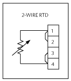
Use a Fluke 724 process calibrator to simulate the RTD. For example, select PT100 RTD as a source and connect Fluke 724 to connector J1 as a 2-wire RTD, Figure 7.
Figure 7. 2-wire RTD connection.
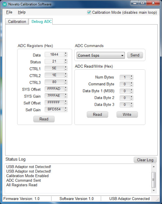
In the Debug ADC tab, select the "Convert 5sps" ADC Command from the pulldown menu, Figure 8.
6.1. Click the "Send" button.
6.2. Click the "Read" button in the ADC Registers group box.
The ADC Registers are read back, Figure 8.
6.3. Click the "0%" button on Fluke 724 to select -200°C.
6.4. Repeat 6.1. and 6.2. The ADC Data register should read 0x50F or something close to that value.
6.5. Click the "100%" button on Fluke 724 to select +800°C.
6.6. Repeat 6.1 and 6.2. The ADC Data register should read 0x6697 or something close to that value.
Manually adjust Self Gain and Self Offset registers until the following ADC Data is read (Table 2).
Table 2. Calibration Points for PT100
Fluke 724 RTD Source
ADC Data (hex)
-200.0°C
50F
0.0°C
1B4E
800.0°C
6697
Tip: For -200°C, start adjusting the Self Offset register until it reaches FFFFFFh value and then continue adjusting the SYS Offset register.
After that, set up 800°C and adjust the Self Gain register starting from the 3rd LSB digit until 6697 is read.
Figure 8. Debug ADC tab.
Step 8: Save to Flash.
Click the "Save To Flash" button in the Calibration tab to store calibration values into nonvolatile memory.
Step 9: Disable Calibration Mode.
Resume normal operation by deselecting the Calibration Mode checkbox.
The Novato reference design fully satisfies the HART physical layer requirements. The HART functions set is developed by AB Tech Solution, an engineering firm specialized in product development services for industrial automation applications.
The HART stack for the Novato reference design supports all universal and common practice commands. The HART stack is not provided by Analog Devices. Contact AB Tech Solution regarding licensing, integration, and further development of device-specific functions.
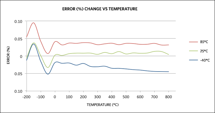
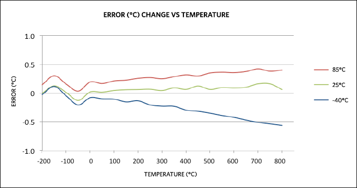
All measurements are taken with the Fluke 724 process calibrator for PT100 RTD. The 4–20mA loop current is measured by the Agilent 34401A digital multimeter as voltage drop over 100Ω load resistor. Measurement results are shown in Figure 9 and Figure 10.
Figure 9. Error (%) change vs. temperature.
Figure 10. Error (°C) change vs. temperature.
The Novato design fits into standard head mounting DIN form B (< 40mm diameter) enclosure.
Note: The Novato calibration software only works with custom made USB-to-UART programming adapter. This adapter is not provided with Novato board and has to be requested separately.
Firmware Files
Firmware is developed using Renesas' e2 studio—complete development and debug environment based on the popular Eclipse CDT project. Use Renesas' E1 Emulator to download firmware through connector J3. The E1 Emulator also provides all the basic debugging function. For more information regarding RL78 MCU, e2 studio IDE, and E1 emulator, refer to Renesas' website.
The Novato reference design comes with firmware loaded on the system.