资源库
Special Considerations for Mode Changes During Active Operation of MAX14820/MAX14821 Sensor/Actuator Transceivers
Abstract
The MAX14820/MAX14821 are Analog's first sensor/actuator transceivers designed for IO-Link® device applications. Both transceivers have an on-board C/Q driver that can be adjusted via the SPI™ interface during active operation. However, there are some special considerations that must be taken into account to avoid falsely detecting a wake-up event. This application note discusses those considerations.
The IO-Link Wake-Up Protocol
In an IO-Link system, communication between a master and a device is point-to-point, with the master sending a request message and the device responding to it. During startup, the IO-Link master initiates a special wake-up current pulse that lasts from 30µs to 160µs to initiate communication with the device, while auto-adjusting the data transmission rate and checking the device identification.
The MAX14820/MAX14821 are Analog's first sensor/actuator transceivers designed for IO-Link device applications. In these applications, the MAX14820/MAX14821 act as the physical layer interface to a microcontroller running the data-link layer protocol. The transceivers detect IO-Link wake-up requests from an IO-Link master on the C/Q line and, in turn, generate a wake-up signal to the microcontroller using the active-low wake-up output pin (/WU\) output.
Normal Wake-Up Detection
The MAX14820/MAX14821 can detect a wake-up request from an I/O Link master when the C/Q line is shorted for 80µs (typ) in any of the programmable output modes (push-pull, PNP, or NPN). The /WU\ output pulses low for 190µs (typ) when a valid wake-up pulse is detected on the C/Q line, signaling to the microcontroller that a wake-up request has been received. Wake-up detection is functional as long as the C/Q driver is enabled.
Figure 1 shows normal wake-up functionality with C/Q in push-pull mode. The master holds the C/Q line during a TX_ pulse, triggering a wake-up pulse on the MAX14820/MAX14821. As shown here, the devices generate a pulse on the /WU\ output when a wake-up event is detected.
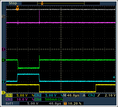
Figure 1. Valid wake-up detection in push-pull mode (R1 = TXEN, CH3 = C/Q, CH4 = current out of C/Q, CH2 = TXC = TXQ, CH1 = /WU\).
Special Considerations
In some cases, the MAX14820/MAX14821 may generate an unexpected wake-up pulse on the /WU\ output if the C/Q line is held high or low, due to downstream circuitry or a large line capacitance. One example of this might occur during a C/Q mode change. Figure 2 shows a situation when an unexpected wake-up might occur. C/Q is changed from push-pull to NPN mode using the SPI interface. The TX_ logic goes high for the wake-up request duration, but the C/Q line voltage drops very slowly due to a large capacitance on the line. The C/Q voltage does not fall below the 8V (min) driver output voltage low threshold during the TX_ pulse and falsely indicates that a wake-up event has occurred.
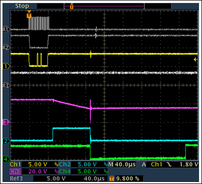
Figure 2. Unexpected wake-up pulse on active-low WU when changing from push-pull to NPN mode (R1 = SCLK, R2 = /CS\, CH1 = SDI, R3 = TXEN, CH3 = C/Q, CH2 = TXC = TXQ, CH4 = /WU\).
The wake-up detection circuitry on the MAX14820/MAX14821 cannot be disabled while the C/Q driver is enabled. However, some simple hardware or software adjustments can negate the effect of the wake-up detect during mode transitions.
A purely software response is to program the controller to ignore pulses on the /WU\ output immediately following a mode change, giving the line time to discharge before acknowledging wake-up events as valid.
To actually disable an unexpected wake-up pulse during this period requires a solution that includes both hardware and software changes. The C/Q driver can be enabled through either the TXEN input pin or by setting the C/QDEn bit in the CQConfig register, so both of these controls must be disabled during a mode change. To do this, follow the steps below:
- Pull the TXEN input pin low.
- Set the C/QDEn bit to 0.
- Change the C/Q transceiver mode.
- Wait before turning the transceiver on again (either by pulling TXEN high or by setting C/QDEn to 1). Calculate the required wait time, tDISCHARGE, following a mode transition using the following equation:
tDISCHARGE = CLINE × (VCC - 8V)/[IDISCHARGE]
where CLINE is the maximum expected capacitance on the C/Q line, and IDISCHARGE is the discharge rate of the line capacitance. If the C/Q driver is in a high-impedance state immediately following the mode transition, then IDISCHARGE is the weak pulldown current on the C/Q pin (100µA (min), 400µA (max)). To decrease the discharge delay, it is also possible to enable the 9mA (max) C/Q load current, disabling the load when the driver is re-enabled.
Figure 3 shows an example of a mode transition on C/Q while a large capacitance downstream on the C/Q line discharges. The C/QDEn bit is set to 0 during the mode-change software command and TXEN pulses low until after all expected TX_ pulses are finished. The C/Q driver is enabled again by pulling TXEN high after the voltage on the C/Q line has fallen below the 8V (min) threshold. Clearly, the device does not generate a pulse on /WU\ under these conditions.
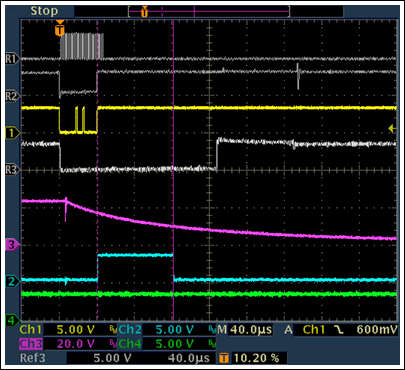
Figure 3. Unexpected wake-up pulse on active-low WU when changing from push-pull to NPN mode (R1 = SCLK, R2 = /CS\, CH1 = SDI, R3 = TXEN, CH3 = C/Q, CH2 = TXC = TXQ, CH4 = /WU\).