Design Note 35: 12-Bit 8-Channel Data Acquisition System Interfaces to IBM PC Serial Port
IBM PCs Collect Analog Data
IBM PC compatibles can be found just about everywhere. In those instances where a PC is not already in place, battery operated portables are readily available. This makes the PC a good choice for controlling a data acquisition system. Typically, such data acquisition systems have been expensive. Using dedicated A/D cards or IEEE-488 controllers and instruments, these systems tie up slots in the PC and are not readily transportable from one machine to another. As an alternative, the schematic of Figure 1 shows a 12-bit, 8-channel data acquisition system that connects to the serial port of the PC. This system uses an LTC1290, a reference, a handful of other low cost components and requires 12 lines of BASIC to transfer data into the PC. If only ten bits of resolution are required the LTC1290 can be replaced with an LTC1090. Additionally, if the LTC1090 is used, the system can be powered directly from the PC serial port with the option shown.
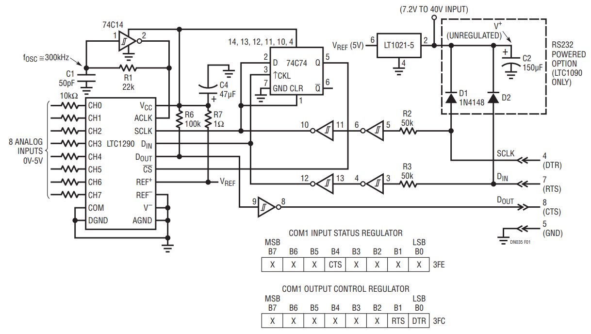
Figure 1. LTC1290 to IBM PC Serial Port Interface.
Two Glue Chips Provide the Interface
The control and status lines of the PC serial port are used to send data to and receive data from the LTC1290. Due to incompatible data formats the Rx and Tx lines are not used. The LTC1290 is a 12-bit, 8-channel data acquisition system on a chip. ACLK of the LTC1290 controls the A/D conversion rate while SCLK controls DIN and DOUT data rates. While CS is low DIN is clocked into the LTC1290 and DOUT is clocked out in a synchronous full duplex format. While CS is high the conversion requested by the last DIN word is performed.
A simple RC oscillator is used to generate ACLK. The DTR pin of the PC serial port is used to form SCLK. The DTR signal is also fed into the CLR and D inputs of a 74C74 so that on the first falling SCLK the Q output of the 74C74 drives the CS of the LTC1290 low. Between data transfers DTR is held high to charge C2 which provides the unregulated V+ if the RS232 powered option is used. V+ is fed into the LT1021 reference which provides a regulated +5V for the LTC1290 and the 74C devices. The RTS pin drives the DIN input of the LTC1290 and the CLK input of the 74C74. During a data transfer, RTS (DIN) changes state only when DTR (SCLK) is low so the 74C74 output (CS) stays low. After the transfer is completed, RTS is toggled while DTR is high causing the Q output (CS of the LTC1290) to go high. DOUT of the LTC1290 goes through an inverter which drives the CTS input of the serial interface. The pull-up resistor on DOUT prevents power consumption in the inverter when DOUT goes into high impedance mode during the conversion.
A Few Lines of BASIC Read the Data
The code of Figure 2 is written in Turbo BASIC. However, this program will run using GW BASIC at about one-third the transfer rate. The addresses used in this program assume that the interface is connected to COM1 of the PC. The LTC1290 is configured by sending the variable DIN$ through the RTS line. DIN$ is a 12-bit string variable which is sent serially LSB first. Bits 11, 10, 9 and 8 are don’t cares and bits zero through seven are the actual LTC1290 DIN word as defined in the data sheet. The following loop is executed twelve times. SCLK and CS are forced low. DIN is set or reset according to the desired word. SCLK is then set high. DOUT is read one bit at a time and multiplied by a weighting variable B, to produce a variable that ranges from 0 to 4095 (0 to 1023 for the LTC1090). The variable B is initialized to 2048 (512 for the LTC1090) and divided by two after each bit. The last time through the loop SCLK is high and DIN is cycled low then high. This causes CS to return high at which time the requested conversion is performed. CS must remain high for 52 ACLK cycles, typically 175μs with the RC oscillator shown. This is not a problem except for the fastest of PCs where a simple FOR…NEXT loop as in line 287 can be used to delay execution of the program until the conversion is complete.
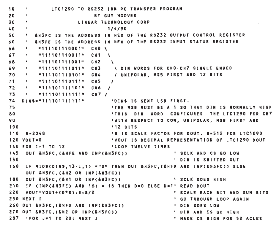
Figure 2. Turbo BASIC Code for LTC1290 to IBM PC Serial Port Interface.
Summary
This interface is capable of performing a conversion and shifting the data in 185ms using an XT compatible running at 4.77MHz. Using a 16MHz 386 the same task can be completed in 2.3ms. The code shown is specifically for the IBM PC and compatibles. However, with the proper software the schematic of Figure 1 should interface with any RS232 port. For a complete description of the LTC1290 and the LTC1090 please see the desired data sheet.
作者
