CN0350
12-Bit, 1 MSPS, Single-Supply, Two-Chip Data Acquisition System for Piezoelectric Sensors


Overview
Design Resources
Design & Integration File
- Schematic
- Bill of Materials
- Gerber Files
- Altium Layout Files
- Assembly Drawing
Evaluation Hardware
Part Numbers with "Z" indicate RoHS Compliance. Boards checked are needed to evaluate this circuit.
- EVAL-CN0350-PMDZ ($58.85) 2-Bit, 1 MSPS, Single-Supply, Two-Chip Data Acquisition System for Piezoelectric Sensors
- EVAL-SDP-CB1Z ($116.52) Evaluation Control Board
- SDP-PMD-IB1Z ($64.74) PMOD to SDP Interposer Board
Device Drivers
Software such as C code and/or FPGA code, used to communicate with component's digital interface.
Features & Benefits
- Two-Chip Piezoelectric Data Acquisition System
- 12-bit, 1MSPS ADC
- Single Supply
Markets and Technologies
Parts Used
Documentation & Resources
-
CN0350 Software User Guide10/16/2018WIKI
-
MT-101: Decoupling Techniques2/14/2015PDF954 kB
-
MT-031: Grounding Data Converters and Solving the Mystery of "AGND" and "DGND"3/20/2009PDF144 kB
-
MT-004: The Good, the Bad, and the Ugly Aspects of ADC Input Noise - Is No Noise Good Noise?3/4/2009PDF342 kB
Circuit Function & Benefits
The circuit shown in Figure 1 is a 12-bit, 1 MSPS data acquisition system utilizing only two active devices.The system processes charge input signals from piezoelectric sensors using a single 3.3 V supply and has a total error of less than 0.25% FSR after calibration over a ±10°C temperature range, making it ideal for a wide variety of laboratory and industrial measurements.
The small footprint of the circuit makes this combination an industry-leading solution for data acquisition systems where accuracy, speed, cost, and size play a critical role.


Circuit Description
The circuit consists of an input signal conditioning stage and an ADC stage. The current input signal is converted to voltage by charge-to-voltage converter (charge amplifier of the U1A op amp and capacitor C2) and amplified by a noninverting amplifier (the U1D op amp and the R7 and R8 resistors). The buffered and attenuated (the U1B and U1C op amps and the resistors R1 and R2) voltage reference (VREF =2.5 V) from the ADC is used to generate an offset HREF of 1.25 V for conditioning the ac signal from sensor to input range of the ADC. Op amps U1A, U1B, U1C, and U1D are one quad AD8608. The output of the U1D op amp is 0.1 V to 2.4 V which matches the input range of the ADC (0 V to 2.5 V) with 100 mV headroom to maintain linearity. Resistor and capacitor values can be modified to accommodate other sensor ranges as described in this circuit note.
The circuit design allows single supply operation. The minimum output voltage specification of the AD8608 is 50 mV for a 2.7 V power supply and 290 mV for 5 V power supply with 10 mA load current, over the temperature range of −40°C to +125°C. A minimum output voltage of 45 mV to 60 mV is a conservative estimate for a 3.3 V power supply, a load current less than 1 mA, and a narrower temperature range.
Considering the tolerances of the parts, the minimum output voltage (low limit of the range) is set to 100 mV to allow for a safety margin. The upper limit of the output range is set to 2.4 V in order to give 100 mV headroom for the positive swing at the ADC input. Therefore, the nominal output voltage range of the input op amp is 0.1 V to 2.4 V.
The AD8608 is chosen for this application because of its low bias current (1 pA maximum), low noise (12 nV/√Hz maximum) and low offset voltage (65 μV maximum). Power dissipation is only 15.8 mW on a 3.3 V supply.
A single-pole RC filter (R6/C8) follows the op amp output stage to reduce the out-of-band noise. The cutoff frequency of the RC filter is set to 664 kHz.
The AD7091R 12-bit 1 MSPS SAR ADC is chosen because of its ultra-low power 349 μA at 3.3 V (1.2 mW) which is significantly lower than any competitive ADC currently available in the market. The AD7091R also contains an internal 2.5 V reference with ±4.5 ppm/°C typical drift. The input bandwidth is 7.5 MHz, and the high speed serial interface is SPI compatible. The AD7091R is available in a small footprint 10-lead MSOP.
The total power dissipation of the circuit is approximately 17 mW when operating on a 3.3 V supply.
The AD7091R requires a 50 MHz serial clock (SCLK) to achieve a 1 MSPS sampling rate. In most piezoelectric sensor applications, a lower sampling rate can be used. The test data taken in this circuit note used an SCLK of 30 MHz and a sampling rate of 300 kSPS.
The digital SPI interface can be connected to the microprocessor evaluation board using the 12-pin PMOD-compatible connector (Digilent PMOD Specifications).
Circuit Design
The circuit shown in Figure 2 converts the input charge to voltage and level shifts to the ADC input range of 0.1 V to 2.4 V.


Piezoelectric elements are commonly used for the measurement of acceleration and vibration. Here, the piezoelectric crystal is used in conjunction with a seismic mass m. If the mass is subjected to an acceleration a, then there is a resulting inertial force F = m × a acting on the seismic mass and the piezoelectric crystal. This results in the crystal acquiring a charge q = d × F, where d (measured in coulombs/newton, C/N) is the crystal charge sensitivity to force.
The resulting steady-state charge sensitivity Sa of piezoelectric accelerometer is Sa = Δq/Δa (measured in C × s2/m).
Note that acceleration can be converted to g using the relationship 1 g = 9.81 m/s2.
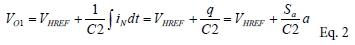
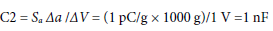
If the accelerometer is used with a charge amplifier with feedback capacitance C2, as is shown in Figure 2, the voltage developed across C2 due to a charge Δq is ΔV = Δq/C2. The corresponding steady state voltage sensitivity is:

The first stage of the signal conditioning circuit in Figure 1 is a charge amplifier (U1A and capacitor C2), where the output voltage is changing corresponding to Equation 1. The output of the circuit is shifted to handle bipolar input signals (for example, vibration measurements). The zero of the circuit is shifted to the middle of the input range of the ADC, using a reference of 1.25 V. The output voltage of the charge amplifier is:
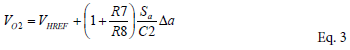
The second stage of the signal conditioning circuit in Figure 1 is a non-inverting amplifier with an output voltage of:
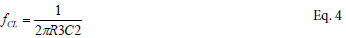
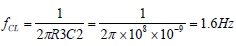
The resistor R3 (100 MΩ to 10 GΩ for ceramic sensors and 10 GΩ to 10 TΩ for crystal sensors) provides dc feedback for the op amp and supplies the input bias current. This resistor must be as small as possible for the minimum frequency measured and determines the lowest limit of frequency input range. At low frequency, the corner frequency fCL is approximately
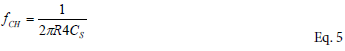
Adding a resistor R4 (1 kΩ to 10 kΩ) in series with the op amp inverting input improves stability and limits input currents due to accidental high input voltage. Increasing R4 further leads to a reduction in the high frequency response. At high frequency R4 may be comparable to the impedance ZS of the sensor (1/ωCS, where CS is the capacitance of the piezoelectric sensor).
The high frequency corner frequency fCH is:
Using Equation 1 to Equation 5, the parameters of the circuit (C2, R7, R8, fCL, and fCH) can be calculated for a specific application.
For example, the Kistler type 8002K quartz accelerometer has the following specifications:
- Range, ±1000 g
- Sensitivity, 1 pC/g
- Capacitance, 90 pF typical
- Frequency Response, −1%, +5% ≈0 Hz to 6000 Hz
- Insulation Resistance, >1013Ω
For an output voltage swing at VO1 of ±1 V, Equation 1 is used to calculate C2.
For an ADC input voltage swing of 0.1 V to 2.4 V (1.25 V ± 1.15 V), the gain of noninverting amplifier has to be equal to 1.15, and the ratio R7/R8 = 0.15. Choose a standard value resistor for R7 =10 kΩ, then R8 = 66.67 kΩ.
Choose R3 = 100 MΩ and neglect the input resistance of the op amp and insulation resistance of the piezoelectric sensor. The corner frequency at low frequency is (see Equation 4)
Choosing R4 =1 kΩ, the corner frequency at high frequency is (see Equation 5)

Thus, the protecting resistor R4 = 1 kΩ does not affect the high pass frequency response because the upper frequency response of the sensor is only 6 kHz.
From Equation 3, the gain of the signal conditioning circuit is

The relative gain error is,

Using the logarithmic derivative principle,
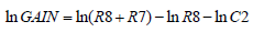
Taking the derivative of lnGAIN,

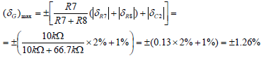
Using 1% tolerance devices R7, R8 and C2, the summing gain error can be estimated.
Worst case relative gain error:
Mean square error (root-sum-square error):

From Equation 3, the output offset of the signal conditioning circuit is
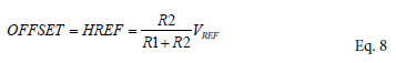
and the relative offset error is

For 1% tolerance of R1, R2, and VREF, the summing offset error can be estimated.
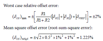
The errors, caused by the tolerances of the resistors, the offsets of the AD8608 op amps (75 μV), and the ADC AD7091R, are eliminated after calibration procedure. It is still necessary to calculate and verify that the U1D op amp output is within the required range (0.1 V to 2.4 V).
Gain and Offset Error due to Temperature Drift of Resistors and Voltage Reference
Using Equation 7 and Equation 9, the errors due to the temperature drift of components can be calculated. For example, for ±100 ppm/°C temperature drift of resistors and for ±25 ppm/°C drift for reference voltage the worst case gain error is less than ±0.013%/°C, and the worst case offset error is about ±0.01%/°C, which corresponds to a worst case total error of less than ±0.25% for ±10°C temperature changes.
Effect of Active Component Temperature Coefficients on Overall Error
The dc offsets of the AD8608 op amps (75 μV) and the AD7091R ADC are eliminated by the calibration procedure.
The offset drift of the AD7091R internal reference is 4.5 ppm/°C typical and 25 ppm/°C maximum.
The offset drift of the AD8608 op amp is 1.5 μV/°C typical and 6 μV/°C maximum.
Note that resistor drift is the largest contributor to total drift if 100 ppm/°C resistors are used, and the drift due to active components can be neglected.
Calibration and Test
Test the sensitivity of a charge amplifier before interfacing it with the sensor so that the gain in the system can be calibrated. An electronic calibration system that does not require application of any mechanical load (acceleration, force, pressure, etc.) is shown in Figure 3. An adjustable amplitude and frequency low impedance output voltage source in series with the calibration capacitor CCAL drives the charge input. The output of the voltage source must be floating with respect to the circuit board ground so that it can operate at the HREF common-mode voltage of 1.25 V.

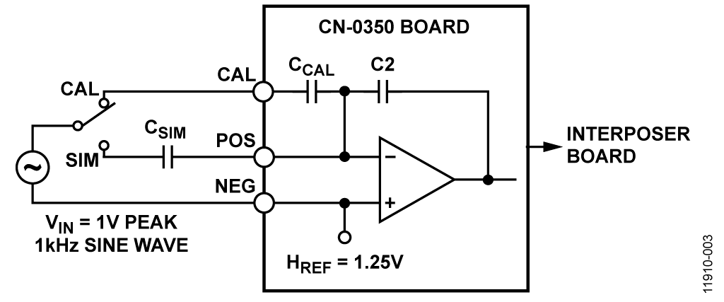
The amount of input charge is Q = CCAL × VIN. For example, an input sine wave voltage with 1 V amplitude and a 1 nF calibration capacitor produces a peak charge input of ±1000 pC. This can be used to calibrate the system. It is important that a 1% tolerance or better capacitor is selected for CCAL to minimize errors. Note that the tolerance of CCAL affects the calibration accuracy. The tolerance of C2 is responsible for the output range, however the temperature change of C2 affects accuracy.
The circuit can then be checked and adjusted using an external simulation capacitor CSIM. Another way to check the circuit is to use the CAL input and an adjustable voltage source. For calibration and simulation purposes, the capacitor CCAL can be changed by connecting an external parallel capacitor with the appropriate value and accuracy across TP1 and TP2. For other input ranges the capacitor C2 can be changed by connecting an external parallel capacitor with appropriate value and accuracy across TP3 and TP4.
Figure 4 shows the measured ADC output for a 1V 1 kHz sine wave input and CSIM = 1 nF. The charge input is therefore ±1000 pC.


Figure 5 shows the actual output using a Loudity LD-BZPN-2312 Piezoelectric Sensor with excitation from a loudspeaker with about 120 Hz sine wave vibrations. The circuit was calibrated with a peak input sine wave voltage of 1 V and CCAL = C2 = 10 nF.


Printed Circuit Board (PCB) Layout Considerations
In any circuit where accuracy is crucial, it is important to consider the power supply and ground return layout on the board. The PCB must isolate the digital and analog sections as much as possible. The PCB for this system was constructed in a simple 2-layer stack up, but a 4-layer stack up will give better EMS. See the MT-031 Tutorial for more discussion on layout and grounding and the MT-101 Tutorial for information on decoupling techniques. The power supply to AD8608 must be decoupled with 10 μF and 0.1 μF capacitors to properly suppress noise and reduce ripple. The capacitors must be placed as close to the device as possible with the 0.1 μF capacitor having a low ESR value. Ceramic capacitors are advised for all high frequency decoupling. Power supply lines must have as large trace width as possible to provide low impedance path and reduce glitch effects on the supply line.
High impedance circuits for conditioning piezoelectric sensor output require attention to resistors, insulation (dielectrics), and cabling. The low impedance input circuit of the charge amplifier significantly reduce the cabling problems, but the requirements on the resistors, insulators, and layout of electrometer amplifiers can also be applied to charge amplifiers built from discrete components. A guard ring around the sensitive input terminals on both sides of printed circuit boards is recommended to minimize input leakage currents . The guard encircles the positive terminal and connects to the reference (common) voltage HREF.
A complete documentation package including schematics, board layout, and bill of materials (BOM) can be found at www.analog.com/CN0350-DesignSupport.
Common Variations
The circuit is proven to work with good stability and accuracy with the component values shown. Other precision op-amps and other ADCs can be used in this configuration to convert ±1000 pC input charge range to digital output and for other various applications for this circuit.
The circuit in Figure 1 can be designed for other than ±1000 pC input charge ranges, following the equations given in the Circuit Design section. The connectors TP3 and TP4 can be used to put additional capacitance in parallel to C2 to build circuits for other ranges. The connectors TP1 and TP2 can be used to put additional capacitance in parallel to CCAL to calibrate the circuit for other ranges.
The AD7091 is similar to the AD7091R, but without the voltage reference output, and the input range is equal to the power supply voltage. The AD7091 can be used with an ADR3425 2.5 V reference. The ADR3425 does not require buffering, therefore a single AD8605 and dual AD8606 can be used in the circuit.
The ADR3425 is a precision 2.5 V band gap voltage reference, featuring low power and high precision (8 ppm/°C of temperature drift) in a 6-lead SOT-23 package.
The AD8601, AD8602 and AD8604 are single, dual, and quad rail-to-rail, input and output, single-supply amplifiers featuring very low offset voltage and wide signal bandwidth, that can be used in place of AD8605, AD8606, and AD8608.
The AD7457 is a 12-bit, 100 kSPS, low power, SAR ADC, and can be used in combination with the ADR3425 voltage reference in place of AD7091R, when a higher throughput rate is not needed.
Circuit Evaluation & Test
This circuit uses the EVAL-CN0350-PMDZ circuit board, the SDP-PMD-IB1Z and the EVAL-SDP-CB1Z system demonstration platform (SDP) evaluation board. The interposer board SDP-PMD-IB1Z and the SDP board EVAL-SDP-CB1Z have 120-pin mating connectors. The interposer board and the EVAL-CN0350-PMDZ board have 12-pin PMOD matching connectors, allowing quick setup and evaluation of the performance of the circuit. The EVAL-CN0350-PMDZ board contains the circuit to be evaluated, as described in this note and the SDP evaluation board is used with the CN0350 evaluation software to capture the data from the EVAL-CN0350-PMDZ circuit board.
Equipment Needed
- PC with a USB port, Windows® XP or Windows Vista® (32-bit), or Windows® 7/8 (64-bit or 32-bit)
- EVAL-CN0350-PMDZ circuit evaluation board
- EVAL-SDP-CB1Z SDP evaluation board
- SDP-PMD-IB1Z interposer board
- EVAL-CFTL-6V-PWRZ power supply
- CN0350 evaluation software
- Precision voltage generator
Getting Started
Load the evaluation software by placing the CN0350 evaluation software disc in the CD drive of the PC. You also can download the most up to date copy of the evaluation software from CN0350 evaluation software. Using My Computer, locate the drive that contains the evaluation software disc and open the file setup.exe. Follow the on-screen prompts to finish the installation. It is recommended to install all software components to the default locations.
Functional Block Diagram
Figure 6 shows the functional diagram of the test setup.
Setup
- Connect the EVAL-CFTL-6V-PWRZ (+6 V dc power supply) to SDP-PMD-IB1Z interposer board via the dc barrel jack
- Connect the SDP-PMD-IB1Z (interposer board) to the EVAL-SDP-CB1Z SDP board via the 120-pin CON A connector
- Connect the EVAL-SDP-CB1Z (SDP board) to the PC via the USB cable
- Connect the EVAL-CN0350-PMDZ evaluation board to the SDP-PMD-IB1Z interposer board via the 12-pin header PMOD connector
- Connect the voltage generator to the EVAL-CN0350-PMDZ evaluation board via terminal block J1Test
Launch the evaluation software. The software is able to communicate to the SDP board if the Analog Devices system development platform drivers are listed in the device manager. Once USB communications are established, the SDP board can be used to send, receive, and capture serial data from the EVAL-CN0350-PMDZ board. Data can be saved in the computer for various values of input voltages. Information and details regarding how to use the evaluation software for data capturing can be found at CN0350 Software User Guide.
A photo of the EVAL-CN0350-PMDZ board is shown in Figure 7.


