CN0337


Overview
Design Resources
Design & Integration File
- Schematic
- Bill of Materials
- Gerber Files
- Altium Files
- Assembly Drawing
Evaluation Hardware
Part Numbers with "Z" indicate RoHS Compliance. Boards checked are needed to evaluate this circuit.
- EVAL-CN0337-PMDZ ($47.08) 2-Bit, 300 kSPS, Single-Supply, Fully Isolated RTD Temperature Measurement System with 3-Wire Compensation
- EVAL-SDP-CB1Z ($116.52) Eval Control Board
- SDP-PMD-IB1Z ($64.74) PMOD to SDP Interposer Board
Device Drivers
Software such as C code and/or FPGA code, used to communicate with component's digital interface.
Features & Benefits
- Flexible RTD Conditioning and Conversion
- Temperature Compensated
- Fully Isolated
Product Categories
Markets and Technologies
Parts Used
Documentation & Resources
-
CN0337 Software User Guide10/12/2018WIKI
-
MT-101: Decoupling Techniques2/14/2015PDF954 kB
Circuit Function & Benefits
The circuit shown in Figure 1 is a completely isolated 12-bit, 300 kSPS RTD temperature measuring system that uses only three active devices. The system processes the output of a Pt100 RTD and includes an innovative circuit for lead-wire compensation using a standard 3-wire connection. The circuit operates on a single 3.3 V supply. The total error after room temperature calibration is less than ±0.24% FSR for a ±10°C change in temperature, making it ideal for a wide variety of industrial temperature measurements.
The small footprint of the circuit makes this combination an industry-leading solution for temperature measurements where accuracy, cost, and size play a critical role. Both data and power are isolated, thereby making the circuit robust to high voltages and also ground-loop interference often encountered in harsh industrial environments.
The novel circuit for 3-wire RTD lead wire compensation was developed by Hristo Ivanov Gigov, Associate Professor and PhD, and Stanimir Krasimirov Stankov, Engineer and PhD Student, Department of Electronic Engineering and Microelectronics, Technical University of Varna, Varna, Bulgaria.


Circuit Description
The input stage of the circuit is an RTD signal conditioning circuit using a compensated 3-wire connection to the RTD. The circuit translates the RTD input resistance range (100 Ω to 212.05 Ω for a 0°C to 300°C temperature range) into voltage levels compatible with the input range of the ADC (0 V to 2.5 V).
The excitation current for the RTD is supplied by op amp U1C that is one-fourth of the quad AD8608. A reference voltage, VR, of 100 mV is developed by the R8/R9 divider driven by the 2.5 V ADC reference. This in turn produces an RTD excitation current of VR/(R1||R2), approximately 1.05 mA.
The excitation current produces a voltage change of approximately 117.6 mV (105 mV to 222.6 mV) across the RTD for a temperature change of 0°C to 300°C. The U1A op amp amplifies this voltage change by 19.6, producing an output span of 2.3 V. Resistor R2 added in parallel with Resistor R1 shifts the output range so that the U1A op amp output is 0.1 V to 2.4 V, which matches the input range of the ADC (0 V to 2.5 V) with 100 mV headroom to maintain linearity. The resistor values can be modified to accommodate other popular temperature ranges as described later in this circuit note.
The circuit design allows single supply operation. The minimum output voltage specification for the AD8608 is 50 mV for a 2.7 V power supply and 290 mV for a 5 V power supply with 10 mA load current, over the temperature range of −40°C to +125°C. A minimum output voltage of 45 mV to 60 mV is a conservative estimate for a 3.3 V power supply, a load current of less than 1 mA, and a narrower temperature range.
Considering the tolerances of the parts, the minimum output voltage (low limit of the range) is set to 100 mV to allow for a safety margin. The upper limit of the output range is set to 2.4 V in order to give 100 mV headroom for the positive swing at the ADC input. Therefore, the nominal output voltage range of the op amp is 0.1 V to 2.4 V.
The op amp U1B is used to buffer the internal 2.5 V voltage reference of the AD7091R (U3) ADC.
The quad AD8608 op amp is chosen for this application because of its low offset voltage (75 μV maximum), low bias current (1 pA maximum), and low noise (12 nV/√Hz maximum). Power dissipation is only 18.5 mW on a 3.3 V supply.
The U1D op amp provides the 3-wire correction signal that compensates for the errors produced by the lead resistances r1 and r2. The gain from Point A to TP1 is +19.6, and the gain from Point B to TP1 is −39.2. The voltage at Point A includes a positive error term that is equal to the voltage dropped across r1 and r2. The voltage at Point B contains a positive error term equal to the voltage dropped across r2, neglecting the small drop across r3. Because the gain from Point B to TP1 is negative and twice the gain from Point A to TP1, the errors due to the voltages dropped across r1 and r2 are cancelled, assuming that r1 = r2.
A single-pole RC filter (R11/C9) follows the op amp output stage to reduce the out-of-band noise. The cutoff frequency of the RC filter is set to 664 kHz. Additional second order filters (adding capacitors C10 and C11) are used for reducing the filter cutoff frequency in case of low frequency industrial noise. In this case, AD7091R is not operating at maximum throughput rate. To increase the conversion speed C10 and C11 should be left unpopulated.
The AD7091R 12-bit 1 MSPS SAR ADC is chosen because of its ultralow power 349 μA at 3.3 V (1.2 mW) which is significantly lower than any competitive ADC currently available in the market. The AD7091R also contains an internal 2.5 V reference with ±4.5 ppm/oC typical drift. The input bandwidth is 7.5 MHz, and the high speed serial interface is SPI compatible. The AD7091R is available in a small footprint 10-lead MSOP.
The total power dissipation of the circuit (excluding the ADuM5401 isolator) is approximately 20 mW when operating on a 3.3 V supply.
Galvanic isolation is provided by the ADuM5401 (C Grade) quad channel digital isolator. In addition to the isolated output data, the ADuM5401 also provides isolated +3.3 V for the circuit. The ADuM5401 is not required for normal circuit operation unless isolation is needed. The ADuM5401 quad-channel, 2.5 kV isolators with integrated dc-to-dc converter, is available in a small 16-lead SOIC. Power dissipation of the ADuM5401 with a 7 MHz clock is approximately 140 mW.
The AD7091R requires a 50 MHz serial clock (SCLK) to achieve a 1 MSPS sampling rate. However, the ADuM5401 (C-grade) isolator has a maximum data rate of 25 Mbps that corresponds to a maximum serial clock frequency of 12.5 MHz. In addition, the SPI port requires that the trailing edge of the SCLK clock the output data into the processor, therefore the total round-trip propagation delay through the ADuM5401 (120 ns maximum) limits the upper clock frequency to 1/120 ns = 8.3 MHz.
Even though the AD7091R is a 12-bit ADC, the serial data is formatted into a 16-bit word to be compatible with the processor serial port requirements. The sampling period, TS, therefore consists of the AD7091R 650 ns conversion time plus 58 ns (extra time required from data sheet, t1 delay + tQUIET delay) plus 16 clock cycles for the SPI interface data transfer.
TS = 650 ns + 58 ns + 16 × 120 ns = 2628 ns
fS = 1/TS = 1/2628 ns = 380 kSPS
In order to provide a safety margin, a maximum SCLK of 7 MHz and a maximum sampling rate of 300 kSPS is recommended. The digital SPI interface can be connected to the microprocessor evaluation board using the 12-pin Pmod-compatible connector (Digilent Pmod Specifications).


Circuit Design
The circuit shown in Figure 2 converts the RTD resistance change from 100 Ω to 212.05 Ω to an output voltage change of 0.1 V to 2.4 V, which is compatible with the ADC input range. In addition, the circuit removes the errors associated with the wiring resistances r1 and r2.
The transfer function of the circuit in Figure 2 is obtained using the superposition principle:


Calculation of the Gain, Output Offset, and Resistor Values and Tolerances
For temperature range of 0°C to 300°C, the RTD Pt100 resistance range is 100 Ω to 212.05 Ω, and the input resistance change, ΔR, for the circuit in Figure 2 is 0 Ω to 112.05 Ω. Therefore, the gain of the circuit from Equation 3 is:


If this condition is met, R1′ = R0 = 100 Ω at 0°C, and VOUT = 0 V
The output offset of the circuit must now be set to 0.1 V. An easy way to shift the output is to make the resistor R1′ slightly less than R0. Note that this affects the gain proportionally. The output offset of 0.1 V is approximately 4.35% of the total span of 2.3 V, therefore the ratio R1′/R0 must be less than 0.9565. To keep the high output level equal to 2.4 V, the ratio R4/R3 can be proportionally corrected. For example, R4 = 0.9565 × 41.06 × R3 = 39.27 kΩ. Using standard resistors values as shown in Figure 1, the circuit gives a good approximation to the required gain and the output offset. Resistor R1′ is formed by connecting Resistor R2 = 1.91 kΩ in parallel with resistor R1 = 100 Ω.
For any other temperature ranges or for any other temperature sensor (for example Pt200, Pt500, Pt1000, Pt2000) the resistor values must be recalculated as follows:
-
Choose a value for R3 (for example, 1 kΩ), and then make R5 = R6 = 2R3.
-
Choose the excitation current through the sensor IR and then calculate VR = IR × RX_low where RX_low = the resistance of the RTD at the lowest temperature of the range.
-
Choose a value for R9 (for example, R9 = 1 kΩ), and then calculate R8:
where VREF = 2.5 V = ADC reference voltage
-
Calculate A = 0.0435 × (RX_high – RX_low) where
A = a temporary constant needed for this calculation procedure.
RX_high = the resistance of the RTD at the highest temperature of the range -
Calculate R0 = RX_low – A.
-
Calculate R0 = R1 × R2/(R1 + R2) and choose the values for R1 and R2. It is recommended to choose a standard value for R1 that is equal to RX_low, and then calculate R2.
-
Calculate
where B= a temporary constant needed for this calculation procedure.
-
Calculate R4 = B × R3, and ensure that R12 = R4.
Accuracy Analysis
Equation 1 shows that all resistors influence the total error. If these values are chosen carefully, the overall error due to substituting standard value resistors can be made less than a few percent. However, use Equation 1 to recalculate the U1A op amp output for 100 Ω and 212.05 Ω inputs to ensure that the required headroom is preserved. In the actual circuit the nearest available standard resistors values were chosen. The Resistors Rl, R2, R8, and R9 are 0.1%, 25 ppm/°C. The other resistors in the circuit are 1%, 100 ppm/°C: R3, R4, R5, R6, and R12.
The absolute accuracy in this type of circuit is primarily determined by the resistors, and therefore gain and offset calibration is required to remove the error due to standard value substitution and resistor tolerances.
Effect of Resistor Temperature Coefficients on Overall Error
Equation 1 shows that the output voltage is a function of nine resistors: R1, R2, R3, R4, R5, R6, R8, R9, and R12.
The sensitivity of the full-scale output voltage at TP1 to small changes in each of the nine resistors was calculated using a simulation program. The input RTD resistance to the circuit was 212 Ω. The individual sensitivities calculated were SR1 = 1.83, SR2 = 0.09, SR3 = 0.94, SR4 = 0.94, SR5 = 1.35, SR6 = 1.28. SR8 = 0.97, SR9 = 0.96, and SR12 = 0.07. Assuming that the individual tempera-ture coefficients combine in a root-sum-square (rss) manner, then the overall full-scale drift 25 ppm/°C resistors for R1, R2, R8, R9, and 100 ppm/°C resistors for R3, R4, R5, R6, R12 is approximately:

Using 25 ppm/°C resistors for all nine resistors reduces the full-scale drift to approximately 80 ppm/°C, or 0.008% FSR/°C.
The error caused by the tolerances of the resistors, the offset of the AD8608 op amps (75 μV), and the ADC AD7091R is eliminated after the calibration procedure. It is still necessary to calculate and verify that the op amp output is within the required range.
Effect of Active Component Temperature Coefficients on Overall Error
The dc offsets of the AD8608 op amps (75 μV) and the AD7091R ADC are eliminated by the calibration procedure.
The offset drift of the ADC AD7091R internal reference is 4.5 ppm/°C typical and 25 ppm/°C maximum.
The offset drift of the AD8608 op op amp is 1 μV/°C typical and 4.5 μV/°C maximum.
Note that resistor drift is the largest contributor to total drift if 50 ppm/°C or 100 ppm/°C resistors are used, and the drift due to active components can be neglected.
Lead Wire Resistance Compensation
The circuit in Figure 1 realizes full compensation for the lead wire resistances (r1, r2, and r3). However, if there is any mismatch in Equation 3, the lead wires r1 and r2 add errors to the measurement. The third lead wire r3 does not have any effect on the circuit because it is connected to the high impedance input of U1D.
The linearity of the circuit is not affected by the lead wires r1 and r2, even if there is mismatch in Equation 3.
RTD Linearization
The circuit in Figure 1 is linear with respect to the resistance change of the RTD. However, the transfer function of the RTD (resistance vs. temperature) is nonlinear. Therefore, linearization is needed to eliminate the nonlinearity error of the RTD. For systems in which a microcontroller is involved, this linearization is typically done in the software. The AN-709 Application Note discusses some linearization techniques for Pt100 RTD sensor. The same techniques are used in the CN0337 evaluation software to eliminate the nonlinearity error of the Pt100 sensor.
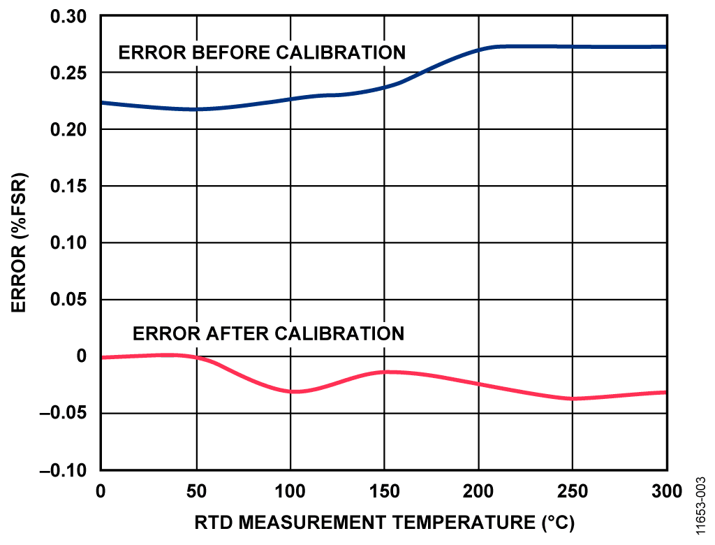
Test Data Before and After Two-Point Calibration
To perform the two-point calibration, a 100 Ω precision resistor is first applied to the input, and the ADC output code is recorded as Code_1. Then a 212.05 Ω precision resistor is applied to the input, and the ADC output code is recorded as Code_2. The gain factor is calculated by

The graph in Figure 3 shows test results for few tested boards before and after calibration (without temperature changes). As it is shown, the maximum error before calibration is about 0.27% FSR. After calibration, the error decreases to ±0.037% FSR, which approximately corresponds to 1.5 LSB error of the ADC.

PCB Layout Considerations
In any circuit where accuracy is crucial, it is important to consider the power supply and ground return layout on the board. The PCB should isolate the digital and analog sections as much as possible. The PCB for this system was constructed in a simple 2-layer stack up, but 4-layer stack up gives better EMS. See the MT-031 Tutorial for more discussion on layout and grounding and the MT-101 Tutorial for information on decoupling techniques. Decouple the power supply to AD8608 with 10 μF and 0.1 μF capacitors to properly suppress noise and reduce ripple. Place the capacitors as close to the device as possible, with the 0.1 μF capacitor having a low ESR value. Ceramic capacitors are advised for all high frequency decoupling. Power supply lines should have as large trace width as possible to provide low impedance path and reduce glitch effects on the supply line. The ADuM5401 isoPower integrated dc-to-dc converter requires power supply bypassing at the input and output supply pins. Note that low ESR bypass capacitors are required between Pin 1 and Pin 2 and between Pin 15 and Pin 16, as close to the chip pads as possible. To suppress noise and reduce ripple, a parallel combination of at least two capacitors is required. The recommended capacitor values are 0.1 μF and 10 μF for VDD1 and VISO. The smaller capacitor must have a lowESR, for example, use of a ceramic capacitor is advised. The total lead length between the ends of the low ESR capacitor and the input power supply pin must not exceed 2 mm. Installing the bypass capacitor with traces more than 2 mm in length may result in data corruption. Consider bypassing between Pin 1 and Pin 8 and between Pin 9 and Pin 16 unless both common ground pins are connected together close to the package. For more information, see ADuM5401 datasheet.
A complete documentation package including schematics, board layout, and bill of materials (BOM) can be found at www.analog.com/CN0337-DesignSupport.
High Voltage Capability
This PCB is designed in adherence with 2500 V basic insulation practices. High voltage testing beyond 2500 V is not recommended. Appropriate care must be taken when using this evaluation board at high voltages, and the PCB should not be relied on for safety functions because it has not been high potential tested (also known as hipot tested or dielectric withstanding voltage tested) or certified for safety.
Common Variations
The circuit is proven to work with good stability and accuracy with component values shown. Other precision op-amps and other ADCs can be used in this configuration to convert resistance deviation input range to digital output and for other various applications of the circuit.
The circuit in Figure 1 can be redesigned for other than 0°C to 300°C input temperature ranges, following the recommendations given in Circuit Design section. Table 1 shows calculations for some standard temperature ranges when using Pt100 RTD sensors.
| Temperature Range | R1 | R2 | R4, R12 | ||
| −50°C to 50°C | 79.4 Ω | 7.82 kΩ | 93.1 kΩ | ||
| 0°C to 50°C | 100 Ω | 11.7 kΩ | 237 kΩ | ||
| 0°C to 100°C | 100 Ω | 5.83 kΩ | 118 kΩ | ||
| 0°C to 200°C | 100 Ω | 2.91kΩ | 59 kΩ | ||
| 0°C to 300°C | 100 Ω | 1.91 kΩ | 39.2 kΩ | ||
| 0°C to 400°C | 100 Ω | 1.45 kΩ | 29.4 kΩ | ||
| 0°C to 500°C | 100 Ω | 1.17 kΩ | 23.7 kΩ | ||
| 0°C to 600°C | 100 Ω | 976 Ω | 19.6 kΩ | ||
| 0°C to 700°C | 100 Ω | 837 Ω | 16.9 kΩ | ||
| 0°C to 800°C | 100 Ω | 723 Ω | 14.7 kΩ | ||
| 1The values for the other resistors are as shown in Figure 1 (R5 = R6 = 2 kΩ, R3 = 1 kΩ, R8 = 26.7 kΩ, R9 = 1.1 kΩ | |||||
The AD7091 is similar to the AD7091R, but without the voltage reference output, and the input range is equal to the power supply voltage. The AD7091 can be used with a 2.5 V ADR391 reference. The ADR391 does not require buffering.
The ADR391 is a precision 2.5 V band gap voltage reference, featuring low power and high precision (9 ppm/°C of temperature drift) in a tiny TSOT package.
The AD8605 and AD8606 are single and dual versions of the quad AD8608 and can be used as a substitute for the AD8608, if different configurations are needed.
The AD8601, AD8602, and AD8604 are single, dual, and quad rail-to-rail, input and output, single-supply amplifiers featuring very low offset voltage and wide signal bandwidth, that can be used in place of AD8605, AD8606, and AD8608.
The AD7457 is a 12-bit, 100 kSPS, low power, SAR ADC, and can be used in combination with the ADR391 voltage reference in place of AD7091R, when a 300 kSPS throughput rate is not needed.
Circuit Evaluation & Test
This circuit uses the EVAL-CN0337-PMDZ circuit board, the SDP-PMD-IB1Z, and the EVAL-SDP-CB1Z system demonstration platform (SDP) evaluation board. The SDP-PMD-IB1Z interposer board and the EVAL-SDP-CB1Z SDP board have 120-pin mating connectors. The interposer board and the EVAL-CN0337-PMDZ board have 12-pin Pmod matching connectors, allowing quick setup and evaluation of the circuit’s performance. The EVAL-CN0337-PMDZ board contains the circuit to be evaluated, as described in this note and the SDP evaluation board is used with the CN0337 evaluation software to capture the data from the EVAL-CN0337-PMDZ circuit board.
Equipment Needed
- PC with a USB port, Windows® XP, Windows Vista® (32- bit), or Windows® 7/8 (64- or 32-bit)
- EVAL-CN0337-PMDZ circuit evaluation board
- EVAL-SDP-CB1Z SDP evaluation board
- SDP-PMD-IB1Z interposer board
- CN0337 evaluation software
- Precision Resistance Decade Box or Pt100 sensor (the calibration procedure can be performed if a resistance box is not available)
Getting Started
Load the evaluation software by placing the CN0337 evaluation software disc in the CD drive of the PC. You also can download the most up to date copy of the evaluation software from CN0337 evaluation software. Using the My Computer icon, locate the drive that contains the evaluation software disc and open the setup.exe file. Follow the on-screen prompts to finish the installation. It is recommended to install all software components to the default locations.
Functional Block Diagram
A functional block diagram of the test setup is shown in Figure 4.


Setup
- Connect the EVAL-CFTL-6V-PWRZ (+6 V dc power supply) to SDP-PMD-IB1Z interposer board via the de barrel jack.
- Connect the SDP-PMD-IB1Z (interposer board) to EVAL-SDP-CB1Z (SDP board) via the 120-pin Connector A.
- Connect the EVAL-SDP-CB1Z (SDP board) to the PC via the USB cable.
- Connect the EVAL-CN0337-PMDZ evaluation board to the SDP-PMD-IB1Z interposer board via the 12-pin header Pmod connector.
- Connect the resistance decade box (Pt100 sensor) to the EVAL-CN0337-PMDZ evaluation board via the terminal block J2.
Test
Launch the evaluation software. The software can communicate to the SDP board if the Analog Devices System Development Platform drivers are listed in the Device Manager. After USB communications are established, the SDP board can be used to send, receive, and capture serial data from the EVAL-CN0337- PMDZ board. Data can be saved in the computer for various values of the input temperature (resistance). Information and details regarding how to use the evaluation software for data capturing can be found at CN0337 Software User Guide.

