Abstract
Patented ADI capacitive programmable gain amplifiers (PGAs) offer better performance than traditional resistive PGAs, including higher common-mode voltage rejection of analog input signals.
This article describes how a chopped capacitive amplifier operates, highlighting the benefits of this architecture when a small signal from the sensor needs to be amplified close to the rails—like in temperature measurements (RTDs or thermocouples) and Wheatstone bridges.
Σ-Δ analog-to-digital converters (ADCs) are widely used in applications with sensors that have small responsivity and reduced bandwidth such as strain gage or thermistors, due to the high dynamic range offered by this architecture. The reason behind the high dynamic range is the low noise performance compared with other ADC architectures.
The Σ-Δ converters base their operation on two principles: oversampling and noise shaping. When an ADC samples the input signal, the quantization noise, which is independent from the sampling frequency, spreads across the entire frequency spectrum up to half of the sampling frequency. Therefore, if the input signal is sampled at a much higher frequency than the minimum dictated by the Nyquist theorem, the quantization noise in the band of interest reduces.
Figure 1 shows an example of the quantization noise density for different sampling frequencies.
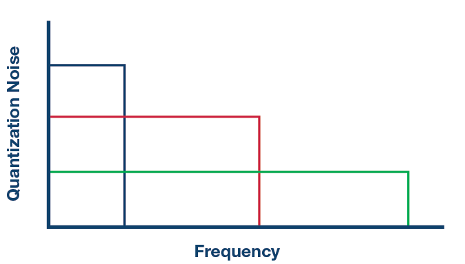
In general and for a given band of interest, the dynamic range improves by 3 dB every oversampling factor of 2 (assuming a white noise spectrum). The second benefit in a Σ-Δ converter is the noise transfer function. It shapes the noise to higher frequencies, as shown in Figure 2, which reduces even more of the quantization noise at the band of interest.
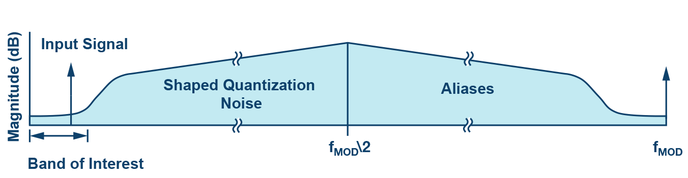
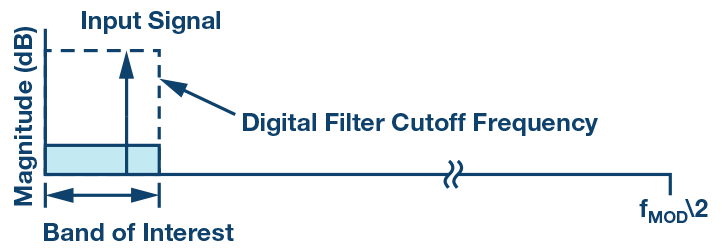
In addition, the Σ-Δ may incorporate a digital filter to remove the quantization noise outside the band of interest, equating to an excellent dynamic range performance, as shown in Figure 3.
Input Buffer
One of the disadvantages of oversampling architectures is that the requirements for an input buffer to drive the Σ-Δ modulator may become more stringent, compared with other architectures that operate at lower sampling frequencies. The acquisition time becomes shorter and, therefore, the buffer requires a higher bandwidth. Modern Σ-Δ converters integrate the input buffer on chip to maximize the ease of use.
Moreover, in sensing systems, presenting a very high input impedance with high precision to the sensing element is critical for the accuracy of the measurement. This makes the requirement for input buffers even more critical.
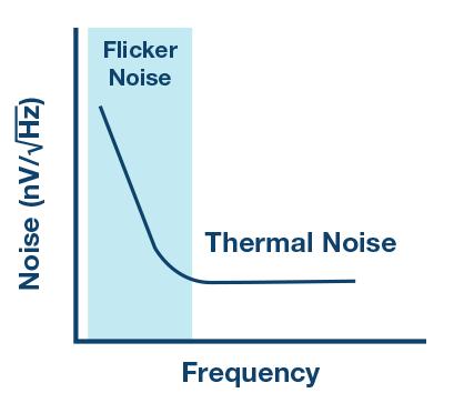
Integrating an input buffer generates other challenges. The Σ-Δ modulator offers very low noise at low frequencies, but any additional components like the input buffer will add thermal noise and, more importantly, flicker noise at low frequencies, as shown in Figure 4.
In addition, the offset of the buffer may contribute to the overall system error. The offset can be compensated by a sys-tem calibration but if the offset drift is relatively high, this approach may become impractical, as it would require that the system be recalibrated every time the temperature of operation changes to compensate the buffer offset contribution.
As an example, when having an offset drift of 500 nV/°C, a 10°C temperature increment will equate into 5 µV offset change, which in a ±2.5 VREF 24-bit ADC, equates to 16.8 LSBs, which is around 4 bits.
The typical way to solve these two problems is by chopping the inputs and outputs of the buffer, as shown in Figure 5.
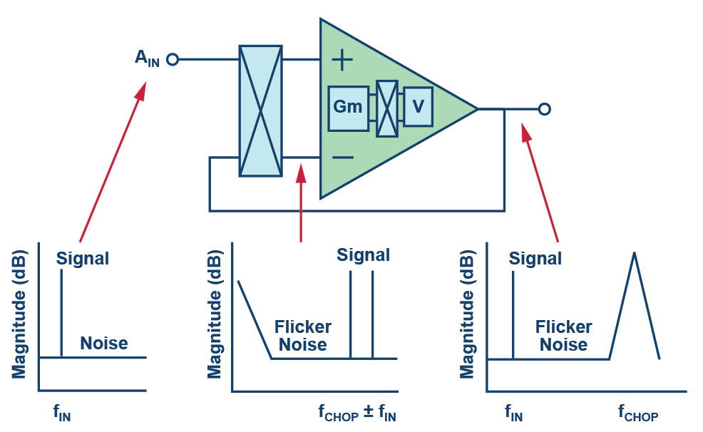
By chopping the inputs, the input frequency is modulated to higher frequencies. The buffer offset and flicker noise remain at their original low frequencies, as they are not affected by the input chopping.
The output dechopper mechanism demodulates the input frequency back to baseband, while it modulates the offset and flicker noise added by the buffer up to higher frequencies that will be removed by the ADC low-pass filter.
In some cases, the input buffers are replaced by a resistor-based instrumentation amplifier (resistive PGA) to accommodate a small sensor signal to the full modulator input range, maximizing the dynamic range. Just note that a resistor-based instrumentation amplifier is preferred over a differential resistive amplifier due to the higher input impedance required in discrete sensors. The resistive PGA implements a similar chopping scheme, as shown in Figure 6.
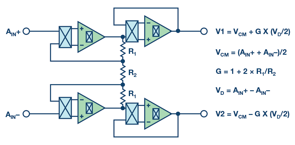
The resistive PGA may require a second set of buffers connected in cascade, as the amplifier may not provide enough bandwidth to drive the modulator directly. Concurrently, the current consumption should be kept low, which dictates the value of the resistors and consequently, the bandwidth of the amplifier.
The main restriction in using this amplifier topology is the limitation on the common-mode voltage, especially with gains other than one, as the resistive PGA has a floating common mode that depends on the input signal, as shown in Figure 6.
Additionally, the resistive network mismatch and its drift is also a concern in the overall error budget, as it may have an impact on most of the precision specifications.
To avoid these limitations, recent ADI Σ-Δ converters have employed a capacitive PGA.
The capacitive PGA amplification principle is similar to the resistive PGA; the gain depends on the capacitor ratios, as shown in Figure 7.
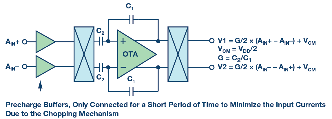
In order to amplify dc signals, the capacitive PGA introduces a chopping mechanism at the PGA inputs, the dc input signal is modulated to the chop frequency, and then it is amplified by the capacitive amplifier. Finally, the signal is demodulated back to dc by the output dechopper. Additionally, the amplifier offset and flicker noise is modulated to the chop frequency and low-pass filtered at a later stage.
There are some benefits associated with this capacitive architecture, as compared with the resistive one:
It offers a better noise vs. power trade-off, as it contains fewer noise sources. Fewer amplifiers are needed and capacitors don’t contribute noise as opposed to the resistors.
Capacitors offer a wide range of advantages over resistors. Apart from being noiseless, they don’t suffer from self-heating and normally offer a better matching and temperature drift. This has a positive impact on offset, gain error, and drift specifications.
The capacitors decouple the input common mode from the rest of the signal chain common mode. This offers an advantage in terms of CMRR, PSRR, and THD.
One of the most powerful advantages is the fact that the capacitive PGA input common-mode range may be rail-to-rail and beyond. That gives the possibility to bias the sensor common-mode voltage pretty much anywhere from the positive rail down to the negative rail.
This capacitive architecture combines the benefits of an instrumentation amplifier in a sense that it has a really high input impedance due to its input being a capacitor. Another benefit of capacitors over resistors as the gain element, is an increase in the dynamic range of the amplifier, not only in terms of signal swing, but also in noise efficiency.
A common solution to overcome the resistive PGA common- mode limitation is to increase or shift the power rails or, alternatively, to recenter the sensor signal common mode. This comes at the expense of higher power consumption, supply design complexity, additional external components, and cost.
Practical Examples
In a Wheatstone bridge, the common-mode voltage is defined by the impedance connected in each of the legs and is proportional to the applied power supply. Weigh scale applications implement this sensing topology due to the benefit of linear sensing in strain gages, Figure 8 shows a half-bridge type II.
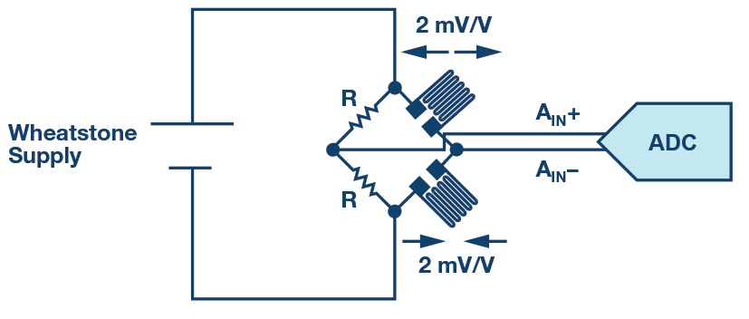
The sensitivity of a strain gage is typically 2 mV/V. The higher the Wheatstone supply, the higher the sensitivity obtained. To increase the dynamic range of the strain gage and maximize the SNR, the bridge may be powered at higher supplies than the ADC.
In a resistive PGA, due to its common-mode limitation, the bridge should be powered at the same supply voltage as the ADC supply in order to maximize the dynamic range, while in a capacitive PGA the bridge can be powered at almost twice the ADC supply voltage as there is no input common-mode limitation.
For example, assuming standard supply levels and powering the ADC at 3.3 V, the improvement of a capacitive PGA over a resistive PGA for the same selected gain can be summarized in Table 1.
Table 1. Comparative of Resistive and Capacitive PGA in a Wheatstone Bridge Assuming Standard Supplies and Gains
| PGA | Resistive PGA |
Capacitive PGA |
| Maximum Wheatstone Supply |
3.3 V |
6 V |
| Strain Gage Differential Sensitivity |
3.3 mV |
6 mV |
| Dynamic Range Improvement (dB) |
5.2 dB |
Another probable issue is a potential difference between grounds when the bridge is connected at some distance from the ADC. This could shift the common-mode voltage, unbalance the ADC input common mode with respect to the bridge, and reduce the maximum allowable gain in the resistive PGA.
A possible way to match the capacitive PGA performance with the resistive PGA is by powering the bridge at a higher supply voltage. For instance, powering the bridge with bipolar supply, ±3.3 V, to increase the sensitivity to the strain gage at the expenses of increased system complexity and power dissipation.
Another case example that could benefit from a capacitive PGA is a temperature measurement using resistance temperature detectors (RTD) or thermocouples.
A popular RTD resistor, such as the PT100, may be used to sense the temperature directly or indirectly sensing the cold junction of a thermocouple, as shown in Figure 9.
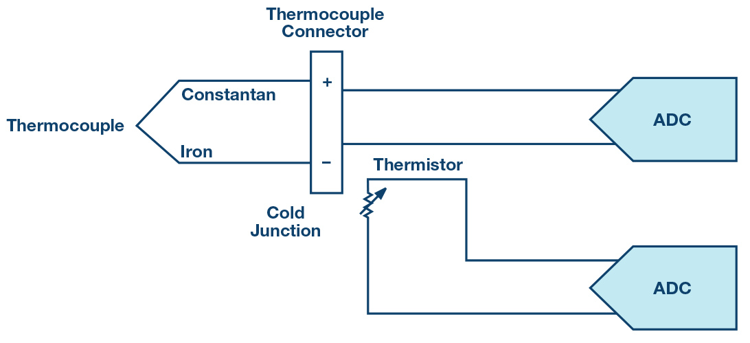
The PT100 is offered with different wires per element, being the most popular and cost-effective 3-wire configuration.
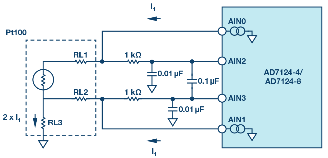
A conventional way to measure the temperature while canceling the lead error is proposed in Figure 10. In this example the internal current sources of the AD7124-8 Σ-Δ ADC with PGA, drive two wires of the RTD with the same current, generating an offset error equal in both leads and proportional to the lead resistance.
Due to the small value of the lead resistance and the currents provided by the AD7174-8 to minimize the self-heating effect, the offset voltage generated in RL3 is close to the negative rail, significantly reducing the maximum allowable gain in a resistive PGA as its input common mode would also be very close to the rails as opposed to a capacitive PGA that will internally set the common-mode voltage to half of the supply rails, allowing for a higher gain configuration and, therefore, increasing the overall dynamic range.
The proposed solution significantly reduces the complexity of the system and the hardware connections, as the third cable should not be returned to the ADC PCB and can be connected to ground near the RTD location.
To increase the precision on the temperature measurement, 4-wire measurements are preferred. In this case, only one current reference is used. To avoid the imprecision on the current source, a ratiometric measurement with a precision resistance used as the ADC reference voltage generator can be used, as shown in Figure 11.
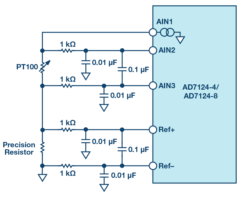
The value of the external precision resistor is chosen so that the maximum voltage generated across the RTD equals the reference voltage divided by the PGA gain.
For a 3.3 V supply, in a resistive PGA, the voltage generated on the precision resistance should be around 1.65 V, otherwise the PGA common-mode voltage will limit the maximum gain. The consequence is that the maximum gained signal should be equal to 1.65 V. In a capacitive PGA, there is no input common-mode limitation, therefore, the RTD common-mode signal can sit close to the top rail, which maximizes the ADC reference voltage generated by the precision resistor, and hence the highest selectable gain and the dynamic range can be maximized.
Table 2 summarizes the maximum gain of a resistive PGA against a capacitive PGA, with a maximum current source of 500 µA to limit the Pt100 self heating, assuming a Class B RTD, at a maximum temperature of 600°C, a maximum VREF of 2.5 V.
Table 2. Comparative of Resistive and Capacitive PGA in a 4-Wire RTD Ratiometric Measurement
| PGA | Resistive |
Capacitive |
| Pt100 Output Voltage |
500 µA × 313.7 = 156.85 mV |
500 µA × 313.7 = 156.85 mV |
| VREF |
1.65 V |
2.5 V |
| Maximum PGA Gain |
1.65 V/156.85 mV ≈ 11 |
2.5 V/156.85 mV ≈ 16 |
| Improvement (dB) | 3.6 |
Conclusion
The capacitive PGA offers an important number of advantages compared with the resistive PGA. Critical specifications such as noise, common-mode rejection, offset, gain error, and temperature drift are improved due to the inherent temperature stability and matching properties of the capacitors as gain elements.
Another key feature is the decoupling of the input common- mode voltage from the amplifier internal common-mode voltage. This is critical when the input signal to be amplified sits on a common-mode voltage close to the rails. The resistive PGA selected gain would be severely restricted by its common- mode limitation, or it would require higher supply rails or external components to rebias the input signal to half of the rails. On the contrary, the capacitive PGA could handle this sensing scenario easily.
Some of the latest Σ-Δ ADC products that include a capacitive PGA are the AD7190, AD7124-4, AD7124-8, and AD7779.

